A computer is a data processing device that consists of a CPU and memory as well as external devices. The CPU is responsible for data processing, the memory is responsible for storage, and the external device is responsible for data input and output, which are connected together by a bus. The CPU is mainly composed of a controller, an operator, and a register. The controller is responsible for reading and scheduling the instructions, the operator is responsible for the execution of the instructions, and the registers are responsible for the storage of the data, which are connected together by the bus in the CPU. Each external device (eg display, hard drive, keyboard, mouse, network card, etc.) consists of a peripheral controller, I/O port, and input and output hardware. The peripheral controller is responsible for the control and operation of the device. The I/O port is responsible for the temporary storage of data, and the input and output hardware is responsible for the specific input and output. They are also connected together by the bus in the external device.
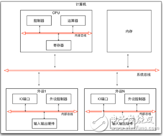
In the above computer system structure diagram, we can see that this componentized design idea of ​​the hardware system is always implemented in all aspects. In this set of design ideas (von Neumann architecture), there is always a part responsible for control, part responsible for execution, part of which is responsible for storage, interaction between it and interface communication is always done through the bus. This kind of design idea can be applied in our software design system: the communication between components and components is decoupled through the way of events, and the internal responsibility of each component needs to be clearly defined within one component (part of which is responsible for scheduling control). Part is responsible for implementing the implementation and part is responsible for data storage).
CacheA complete CPU system has control components, arithmetic components, and register components. The role of the middle register component is to temporarily store data. Since there is memory as a place to store data, why do you still have registers? The answer is speed and cost. We know that the CPU is very fast. If you put the data into the memory, it will greatly reduce the performance of the entire system. The solution is to open a small temporary storage area inside the CPU, and copy the data from the memory to the small temporary storage area when performing the operation, and the operation is performed in this small fast temporary storage area. We call this small temporary storage area a register. Because registers and operators and controllers are very closely linked, their frequency is the same, so the operation will not cause an overall decline in system performance due to the back-and-forth transmission of data and the frequency difference between devices. You may ask why you don't integrate the entire memory into the CPU. The answer is actually a cost issue!
Because the CPU speed is very fast, the corresponding registers also need to be accessed very quickly, and the speeds of the two are matched. Therefore, these registers are difficult to manufacture, the materials are fine, and they are integrated into the chip, and the price is high. The cost of memory is relatively low, and from a technical point of view, it is impossible to integrate a large number of memory cells inside the CPU.
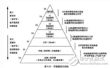
The problem of operation is solved by the register, but there is still a problem: we know that the program is to load all executable binary instruction code into the memory at runtime, and the CPU needs to execute the instruction from the memory before executing one instruction. Read into the CPU and execute. If you read an instruction from memory every time to execute it in order, then there is still a processing bottleneck between the CPU and the memory, resulting in a decline in overall performance. How to solve this problem? The answer is the cache. In fact, there are not only registers designed to solve operational problems inside the CPU, but also a partial cache storage area. The manufacturing cost of the high cache is lower than the register, but it is higher than the manufacturing cost of the memory, and the capacity is larger than the register, but much smaller than the memory. Although there is no such thing as a close distance between the register and the operator, it is much closer than the distance from the memory to the operator. In general, the cache in the CPU may be as large as a few KB or tens of KB. It is through the introduction of the cache that when the program is running, some of the instruction code and data to be executed in the memory can be copied into the cache in advance, and the CPU no longer reads the instruction from the memory every time. Instead, the instructions are executed directly from the cache, which speeds up the overall speed. Of course, it is necessary to pre-read the instructions and data of the memory area to the cache and how to read these tasks to the operating system to complete the scheduling. The algorithm and logic are very complicated. You can learn the operating system. The course to understand, here is no longer open. It can be seen that the role of the cache solves the problem of data transfer between devices of different speeds. In practice, there may be more than one level of cache inside the CPU. It may be equipped with two levels to three levels of cache. The higher the higher the cache speed, the lower the capacity, and the lower the level, the slower the cache. , but the bigger the capacity. For example, the arm processor A11 on the iPhoneX has the capacity of 64KB for the L1 cache and the 8MB for the L2 cache. The L2 cache has a capacity of 8M. When the program code is small, the code can be read into the cache to run at once, and there is no third-level cache.
We know that there is a so-called space-changing concept in software design. When two objects interact with each other because the processing speeds of the two objects are not consistent, we need to introduce a cache to solve the problem of inconsistent reading and writing. For example, when reading or writing a file or socket communication, because the processing speed of the IO device is very slow, it is always necessary to save some data read or written to a cache during file reading and writing and socket communication, and then unify. Perform read and write operations.
It can be seen that whether at the hardware level or at the software level, when the two components cannot interact synchronously due to speed problems, the cache technology can be used to compensate for this imbalance.
Register in the instructionEach instruction executed by the CPU consists of an opcode and an operand. A simple understanding is what to do (operand) (opcode). The data to be calculated inside the CPU is always placed in the register, and the actual data may be placed in the memory or in the IO port. So our program actually does the following three things most of the time:
Read data from memory or I/O port into register
The data in the register is operated (the operation can only be performed in the register)
Write the contents of the register back to the internal memory or I/O port
These three things are related to registers. Registers are the transfer stations for data storage. It is very important. Therefore, in the instructions provided by the CPU, if there are two operands, at least one of them must be a register.
The following section is an example of the arm64 command:
Mov x0, #0x100 ; assign constant 0x100 to register x0
Mov x1, x0 ; assign the value of register x0 to register x1
Ldr x3, [sp, #0x8] ; assign the memory value at the top of the stack plus 0x8 to the x3 register
Add x0, x1, x2 ;x0 = x1 + x2 It can be seen that the instruction of the operation must be placed in the register
Sub x0, x1, x2 ;r0 = x1 - x2
Str x1, [sp, #0x08] ; Saves the value in register x1 to the top of the stack plus the memory at 0x8.
The following section is an example of an x64 instruction (AT&T assembly):
Mov $0x100, %rax ; assign constant 0x100 to register rax
Mov %rax, %rbx ; assign the value of register rax to the rbx register
Movq 8 (%rax), %rbx ; the value in register rax +8 and the data in the pointed memory is assigned to the rbx register
So don't think of machine language or assembly language as a very complicated or incomprehensible language. If you look closely at an assembly language code, you will find that almost all of the code is doing the above three things. What we see in high-level languages ​​is just variables, but in low-level languages ​​we see memory addresses and registers. You can also understand memory addresses and registers as defined variables. With this idea, you can read assembly code when you It will be found that assembly language is not so difficult. In high-level languages, we can define a lot of variables with special meaning according to our own needs, but in low-level languages, because there are several registers, it must be reused and reused, so there will be a lot of will be in assembly language. The contents of the register are saved to the instruction code in memory and the instruction code read from the memory into the register. Many of these codes have commonalities. As long as you read more in your practice, and then adapt to it, you will soon be happy to see the assembly code. Practice makes perfect.
Type1 Tethered Cable,16A Type1 Tethered Cable,32A Type1 Tethered Cable,Type 1 Tethered Charging Cable
Yangzhou JERI New Energy Co., Ltd. , https://www.jrevcharging.com