1, FLASH operating program design
Let's learn the content of programming. Before learning programming, we must first understand the control registers of the FLASH memory module.
All operations of the FLASH memory module are implemented by controlling the associated control registers. Including FCTL1, FCTL2, FCTL3 three control registers, of which FCTL1 mainly contains the control bits for FLASH programming and erasing operations; FCTL2 mainly defines the clock source and frequency division coefficient before entering the timing generator; FCTL3 saves some of the FLASH memory modules Sign bit.
2, FCTL1 control register

FWKEY: The security key value of the FLASH storage module. A total of 8 bits, the corresponding security key value should be written to the FLASH operation, otherwise it will cause the PUC signal and the KEYV signal. 0x96: Security key value when reading; 0x5A: Security key value when writing.
BLKWRT: Segment programming control bit. When you need to program a segment or segments continuously, using segment programming can speed up programming. 1: Use segment programming mode; 0: Do not apply segment programming mode.
WRT: Programming control bit. This bit must be set when programming the FLASH, otherwise the ACCVIFG (Illegal Access Interrupt Flag) bit will be set. 1: Allow FLASH programming; 0: Disable FLASH programming.
MERAS: Multi-segment erase control bit. When multiple segments need to be erased, the pair is set to be set. 1: erase multiple segments; 0: do not erase.
ERASE: But the segment erase control bit, which is set when a segment needs to be erased. 1: Erase one segment; 0: Do not erase.
3, FCTL2 control register

FWKEY: The security key value of the FLASH storage module. A total of 8 bits, the corresponding security key value should be written to the FLASH operation, otherwise it will cause the PUC signal and the KEYV signal. 0x96: Security key value when reading; 0x5A: Security key value when writing.
FSSEL1~0: Select the clock source of the timing generator of the FLASH memory module. 3: Select SMCLK; 2: Select SMCLK; 1: Select CMLK; 0: Select ACLK.
FN5-0: Select the division factor for the clock source of the timing generator. The final division ratio is 32*FN5+16*FN4+8*FN3+4*FN2+2*FN1+FN0+1.
4, FCTL3 control register
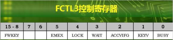
FWKEY is a security key, the same as the first two, we will not go into details.
EMEX: Emergency exit. This bit can be used to stop the operation of FLASH urgently. 1: Emergency stop FLASH operation; 0: No operation.
LOCK: FLASH lock bit. If the FLASH erase and write operations are performed during this bit, illegal access will result, and the corresponding flag bit ACCVIFGF will be set. 1: Lock the FLASH memory module, it can be read when locked, but it cannot be erased and written. 0: The FLASH memory module is not locked, and it can be read, written and erasable.
WAIT: Wait for the flag bit, the user has obtained the FLASH memory and segment programming state by reading the state of this bit. 1: Segment programming is active; 0: Segment programming operation is in progress.
ACCVIFG: Illegal access flag. 1: illegal access; 0: no illegal access.
KEYV: Illegal security key value flag. 1: error security key value; 0: correct security key value.
BUSY: FLASH storage module busy flag. 1: The current FLASH storage module is busy; 0: The current FLASH storage module is idle.
5, single-byte write operation

When writing a single byte in the program, write data 0xAA to address 0x1090 in Seg_A. From this block, we can see that the basic flow of data written to FLASH is mostly similar to erasure. It is important to note that in this procedure we have omitted the link to detect the BUSY status bit, and in actual cases, as long as the user program is not a frequent, cross-operating FLASH memory module, it is generally necessary to detect the BUSY bit.
For multi-byte write operations, the basic operation mode is similar to a single byte, and only needs to modify the FLASH address pointer each time and write the corresponding data.
6, segment erase operation

Although the MSP430 series MCU can write data to any address of the FLASH memory module, the erase operation can only operate in the basic unit of the segment, that is, at least the Seg_A and Seg_B segments can be erased. From the example program, you can see the basic flow of segment erase: in addition to the basic settings before starting the erase operation, the basic settings after the erase, you need to pay special attention to: the segment to be erased (program The median Seg_A) writes arbitrary data to any of the addresses to initiate the erase operation. Again, this is a simplified block and there are no flags such as BUSY.
This is a very classic TI program for FLASH memory modules, which can be seen on almost all books on MSP430. This program contains erase, segment write, segment copy, etc. It is a very good example.
It is important to note that the previous program is just an example. Before you can operate FLASH in a very complicated program, be sure to disable all interrupts and disable the watchdog. Remember to remember.
Organize your cabling
- Organizes all types of cables
- Ideal for network Patch Panel cabling
- Finger duct design allows easy cable organization
- Cable pass-through holes in the back of the duct
- Only set up 1U rack
- Work with threaded, round and square hole racks
- EIA 19" RACK standard compliable
- Including screws and mounting hardware
Metal Cable Management,1U Metal cable management,stainless steel cable management,metal cable tie mount
NINGBO UONICORE ELECTRONICS CO., LTD , https://www.uniconmelectronics.com