Introduction General Purpose Input Output (GPIO) port expander ICs can provide the right amount of I / O ports in a small, low-cost design. Chips that can provide 8 or 16 ports are almost simultaneously related to their I²C and SPI serial buses come out. The functions of early devices mainly include: open-drain output or push-pull output with current limiting drive, and logic input with non-latching transient detection. Can provide TSSOP minimum package.
This application note discusses the latest port extenders. These device functions are closely related to the design of space-constrained and cost-sensitive folding mobile phones. The internal connection of a folding mobile phone is similar to a clam shell, consisting of two shells folded together (Figure 1). The main part is usually half of the thickness, including the baseband circuit, radio frequency circuit, and keyboard, battery, antenna and so on. A common layout of a compact mobile phone is to place a large display inside the cover and a small display outside the cover, as shown. The external screen is usually a semi-reflective LCD, which can be seen clearly even when there is no backlight, and is always on to display the idle state and other information of the mobile phone. There are telephone headsets and other audio and ringing circuits around the cover. Many canopies are also designed with a camera module.
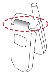
Figure 1. A flexible circuit is used to connect the two parts of the phone, but the hinge for folding the phone is the bottleneck of the internal connection.
In most of the accessories of the cover, the display screen and the camera have a separate parallel interface bus with an appropriate speed (Mbps), which is used to refresh the display screen and download pictures. However, there is a certain bottleneck in transferring data from the cover to the main body through the rotating shaft. The hinge is usually a flexible circuit made of Mylar® and copper wire. In order to ensure the reliability of the circuit after repeated folding, the wiring density (that is, the number of wiring) must be limited. Mobile phone designers must reduce the number of connections between the cover and the body, which increases the design difficulty. The advantages of GPIO port extenders in folding mobile phone applications are usually. The design of folding mobile phones should minimize the number of copper wires connecting the cover and the flexible circuit of the body. The development trend is to serially convert the high-speed parallel connection between the lid display and the camera. A simple way to reduce other wiring is to identify the signal wire and the control wire and synthesize it directly on the cover instead of connecting it through a flexible circuit. The small size and low cost port expander can control logic signal input and output, LED driver or power control switch. The port extender is connected to the motherboard via an I²C or SPI interface, which may be provided on the cover.
The port extender is also a low-power device. If you want to play a role in mobile phone design, the port extender must meet the following conditions: Have a small size package (2mm x 2mm or 3mm x 3mm thin QFN package), so that it can be placed anywhere . It has a standard serial protocol interface, such as I²C or SPI interface. Interrupt the drive to avoid large power consumption caused by CPU polling. The main functions (PWM, input monitoring) can be performed without CPU intervention. Operating at a low supply voltage of 1.8V to 3V, the operating voltage can even be lower than 1V. Power supply current consumption is less than 1µA. LED driver LEDs are used in mobile phones for display and keyboard backlight (2 to 6 LEDs), function or status indication, RGB flashing, and battery and signal strength indication. The port extender can save space, power consumption, and reduce unnecessary operation of the system, mainly in the following aspects: PWM brightness control of a single LED; high voltage, high current drive, no discrete transistors that occupy space; directly powered by battery The LED driver reduces costs and eliminates the EMI of the charge pump or inductor-based boost power supply.
The open-drain port provides high current drive. The open-drain output port is easy to drive an LED. This port is like a hardware output switch that uses a series resistor (commonly called a ballast resistor) to set the LED current. The port expander is very suitable for driving high-current ports with a rated voltage higher than the power supply voltage, and adjusts the LED brightness through a pulse width modulation (PWM) signal. For example, the MAX6965 LED driver provides 9 outputs, with brightness control and hot-plug protection, in a 3mm x 3mm QFN package. The device provides 9 open-drain GPIOs with a rated voltage of 7V, can sink 50mA, and provides independent PWM outputs.
When powered directly by the battery, it can provide constant current port driving for the LED. The ideal LED driving method is a constant current source, which replaces the traditional hardware output switch and current limiting ballast resistance solution. The constant current LED driver has two main advantages: The LED current has nothing to do with the LED forward voltage or the change of the LED power supply voltage. Reducing the LED power supply voltage (close to the LED forward voltage) can improve efficiency. The constant current driver allows a lower LED supply voltage because the voltage across the ballast resistor must be high enough to compensate for changes in the LED supply voltage and forward voltage drop. For example, if a 5V ± 5% power supply is used to drive a white LED, the specified forward voltage is 3.1V ± 0.25V. The nominal value of the voltage across the ballast resistor is 1.9V, with a range of 1.4V to 2.4V. Thus, the maximum change in current is ± 26%. If the power supply voltage drop is 4V ± 3%, the nominal voltage of the ballast resistor is 0.9V, and its variation range is 0.53V to 1.27V. At this time, although the power supply tolerance is reduced, the maximum change in current is ± 41%.
Even if the voltage drop across the output port is higher than the specified minimum (Figure 2), constant current drivers such as the MAX6966 (10-port LED driver and I / O expander with PWM brightness control) can accurately adjust its constant current Output. The port output voltage is the difference between the power supply voltage of the load (usually LED) and the voltage across the load (LED forward voltage). If the LED power supply voltage drops and the minimum port output voltage cannot be maintained, the output stage of the driver will enter a power failure state and the load current will drop accordingly. For the sink current of 10mA, the minimum port voltage of MAX6966 is about 0.5V; for the sink current of 20mA, the minimum port voltage is about 1V.
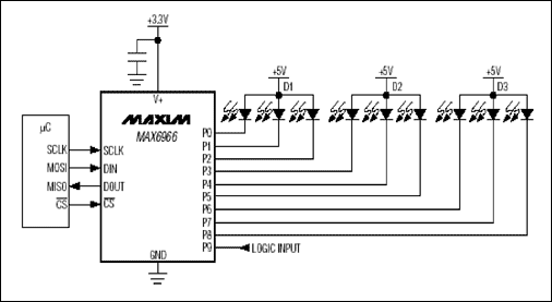
Figure 2. The MAX6966 GPIO IC includes LED drivers and logic I / O ports
When the LED is directly powered by the mobile phone battery, it can save space and save the cost of the boost converter. Therefore, a typical LED power supply is a rechargeable lithium battery. The battery voltage is 4.2V when fully charged, 3.4V to 3.7V in use, and drops to 3V after full discharge. When the battery power supply is insufficient, the LED power supply voltage is significantly lower than the voltage of the power supply failure state.
Figure 3 shows the typical sink current of a 3V blue LED (LITEON LTST-C170TBKT) when the LED power supply voltage changes from 2.5V to 7V. The LED shown in the figure is driven by a constant current port pre-programmed to 10mA and 20mA, and the power supply voltage continuously changes in the range of 2.5V to 7V. It can be seen that the forward voltage of the LED decreases as the current decreases. Therefore, the LED current will slowly decrease when the power fails, rather than directly to the failure state. When the LED power supply voltage drops to 3V, the LED current drops to 6mA or 7mA, which is acceptable for most backlight applications when the battery is depleted.
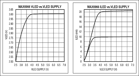
Figure 3. The MAX6966 constant current output directly uses a mobile phone battery to drive the white LED. The traditional PWM control method is that all PWM outputs use the same PWM timing, that is, all outputs are turned on at the same time (Figure 4). Therefore, the LED driver set by PWM will sink the power supply current at the same time. For example, if the duty ratio of all outputs is set to 50:50, then the current sink is zero for half of the time (all loads are off), and the sink current is full for the other half of the time (all loads are on).
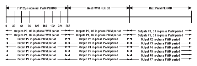
Figure 4. Traditional PWM architecture causes all output ports to switch simultaneously
The PWM output of each port of the MAX6966 constant current LED driver works in a wrong phase, with a difference of 1/8 of the PWM period (Figure 5). The output switching time of each port is evenly distributed during the PWM period, thereby reducing the power output switching transient di / dt And peak / average current, while also reducing EMI, and allows the power supply to use narrower PCB layout.

Figure 5. MAX6966 makes PWM work out of phase, balances the demand for power supply current, and automatically reduces the LED brightness. The automatic control function of MAX6966 allows the current output to gradually decrease to the automatic shutdown state (slow drop), and the current gradually increases when exiting the shutdown state No more operations are required (Figure 6 and Figure 7). The slow-down process includes a programmable delay time, during which the output current remains at the maximum value, and then the current gradually decreases within a preset fade-out time.
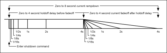
Figure 6. The MAX6966 automatically decreases the LED brightness and gradually weakens after a certain delay
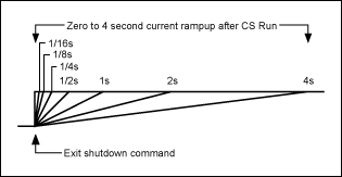
Figure 7. The MAX6966 can be triggered by hardware to control the rate of rise of the LED brightness, so as to obtain a certain time to disconnect unwanted peripherals
In the off state, a short pulse at the CS input can be used to activate the MAX6966. This hardware wake-up feature allows the power management controller or similar ASIC to start the MAX6966 with a preset LED brightness configuration. When exiting the off state, the LED output can automatically rise slowly to the preset current (Figure 7). This design method solves the time management problem of the system processor; it also allows the system to enter standby mode, and the LED driver itself performs the timing function.
Many GPIO devices provide higher source current and sink current, which can be used to turn on or off peripherals when the power supply is directly powered. From this function, you can learn the following application tips: In any application, you should try to control the GND pin of the peripheral device instead of controlling the positive power supply. Load devices that are easily controlled by ground switches include vibration motors, LEDs, and many IrDA interface modules. Grounding switches are preferred because they generally provide high current and open-drain ports. The use of push-pull GPIO (MAX7310, MAX7312, MAX7320) to control the positive power supply of peripheral devices requires a small supply current. This method is commonly used for IC power-down protection. Use an external PFET to extend the high-side current drive of a push-pull GPIO. Simply connect the gate of the PFET to the push-pull output port, connect the source to the positive pole of the power supply, and the drain to the load. It should be noted that the current control logic is reversed: the logic low level of the output port turns on the PFET. Parallel open-drain ports can obtain greater drive current. Make sure the ports are opened and closed at the same time to drive the load together. Port Extender-Simple I / O for level-shifting GPIO has another important function: to switch input and output between high and low voltage. The following is a list of some level-shifting uses: The withstand voltage value of the input port is usually higher than the operating voltage of the GPIO. This feature allows GPIOs working at low power supply voltages to monitor higher voltage logic inputs. The I2C interface can withstand 5.5V, regardless of the operating voltage of the GPIO. Therefore, the I²C bus pulled up to 3.3V through a resistor can communicate with GPIOs operating at 2.5V or 1.8V. Open drain I / O can usually withstand the voltage and GPIO operating voltage. For example, the I / O ports of the MAX6964 / MAX6965 and MAX7313-MAX7316 series can withstand 5.5V or 7V. Connect a pull-up resistor between the port and the required power supply, any port can produce a swing that reaches the specified logic level. Open-drain I / O and I²C interfaces are usually hot-swappable, which means that when the GPIO supply voltage is disconnected, these connections can withstand the applied voltage without the need for additional parasitic current absorption. The hot-swap function is very useful when connected to a separately powered mobile phone accessory, that is, the mobile phone and accessory can be powered on in any order. With a large resistance pull-up resistor (~ 1MΩ), the default level of the push-pull I / O port at power-on can be set to the power supply voltage, or it can be set to ground level by a pull-down resistor. The I / O port defaults to a high-impedance input at power-up, so before programming GPIO through its serial interface, the initial logic level is set by the resistor. Port expansion: Automatic input monitoring As mentioned above, peripherals should be driven by event interrupts to avoid CPU polling. This is particularly important for GPIO inputs that monitor accidental events, such as cell phone flips or power failure alarms. Most GPIOs include transient detection circuits that monitor all logic input changes and generate interrupts when the input state changes. The MAX7319 is an I²C port expander with 8 open-drain I / Os that expands the traditional transient detection function as follows: Latch interrupt output / INT, which will not generate an interrupt until the transient changes when reading the MAX7319 request. After reading the MAX7319, the change flag register can identify any changed ports, even for transient changes. The interrupt mask register only allows a specific input port to trigger an interrupt when it changes. When the input of any port changes, the transient flag of the corresponding port is set; even if the input returns to the original state, the flag remains unchanged. The port interrupt mask bit determines whether an input port that has a transient change generates an interrupt. High-priority input interrupts are enabled by interrupt mask bits. Interrupts allow the system to respond quickly to changes in these input ports. Polling can be used to detect low-priority inputs. The transient flag indicates whether the input port has changed since the last access.
1.ANTENK Flexible Printed Circuit (FPC) and Flexible Flat Cable (FFC) connectors are ZIF (zero insertion force) and LIF (low insertion force) connectors designed to provide a fast, easy, reliable method to make a connection of flexible printed circuits to a PCB. Adam Tech`s special contact design completely preserves conductor integrity by eliminating all wiping action while making connection. Flex circuitry enters the connector and the connector cap is pressed down to capture the flex circuit producing a stable, high pressure connection. Raising the cap releases the pressure for exchange or replacement of circuitry. This series includes single and dual row versions in thru-hole or SMT mounting in vertical or horizontal orientations.
2.Our products are widely used in electronic equipments,such as monitors ,electronic instruments,computer motherboards,program-controlled switchboards,LED,digital cameras,MP4 players,a variety of removable storage disks,cordless telephones,walkie-talkies,mobile phones,digital home appliances and electronic toys,high-speed train,aviation,communication station,Military and so on


FFC Connector Range Available as:
0.3,0.5, 0.8, 1.0,1.25, 2.54mm connector pitch
Surface mount
Side and Top entry
Side entry parts - Top and bottom contact options
ZIF (Zero Insertion Force)
Slide and flip lock actuator styles
Specifications:
Material And Finish:
Insulator: LCP
Lock: PPS
Insert Spring:Phosphor Bronze,
Matte Tin Plated
Solder Platten Area:Phosphor
Bronze,Matte Tin Plated
Voltage:500 V AC(rms)/DC
Current:0.5 A AC(rms)/DC
Contact Resistance:20 mΩ max(initial)
Insulation Resistance:800 MΩ min
Operating Temp:-20°-85°
Fpc Connector,Fpc Cable Connectors,Ffc Cable Connectors,Pitch Fpc Connector,Surface mount FPC/FFC Connectors,Top entry FFC Connectors, Side entry FFC Connectors
ShenZhen Antenk Electronics Co,Ltd , https://www.antenkelec.com