Design of Radio Receiver Module Based on TA31136
0 Introduction Digital communication is widely used in wireless monitoring systems in municipal engineering and industrial fields such as water, electricity, gas, oil, and lamps. Its core part is digital transmission radio. The performance of the digital radio station directly affects the communication quality of the monitoring system, so it is a key device in the monitoring terminal and is also a typical digital communication RF wireless transceiver device. It has more digital communication interfaces than the most common radios. The internal circuit contains almost all the circuits commonly used in radio frequency communication equipment and radio frequency communication system solutions. Therefore, digital radio stations are often used to build wireless radio frequency monitoring systems. In the communication system, the most difficult part to design is the receiver. Because the receiver must have low noise figure, small group delay variation, small intermodulation distortion (IMD), large frequency dynamic range, stable automatic gain control (AGC), appropriate radio frequency (RF) and intermediate frequency (IF ) Gain, good frequency stability, satisfactory gain stability (specifically multi-channel), low phase noise, negligible in-band interference, sufficient selectivity, appropriate bit error rate and other characteristics. At the same time, it may be subject to cost constraints.
1 Receiver scheme Generally speaking, the design scheme of the receiver mainly includes the superheterodyne receiver scheme, direct down conversion scheme and digital zero-IF scheme. The superheterodyne receiver solution has the advantages of easy implementation, high stability and less interference. It is easier to demodulate at a lower fixed intermediate frequency. The disadvantage is that the combined frequency interference is more serious; there is no image interference in the direct down conversion solution. Disadvantages are local oscillator leakage, poor noise performance, and DC offset; the digital zero-IF scheme refers to the process of digitization in the design of the intermediate frequency part of the system, so the signal-to-noise ratio (SNR) can be improved and reliability The disadvantage is the complexity and cost of the system. Considering that this digital radio station mainly works in the field environment, which requires strong anti-interference and anti-noise capabilities, as well as miniaturization and low cost, therefore, the superheterodyne receiver solution is the most suitable.
Superheterodyne receivers generally use intermediate frequency in signal processing, so they are also called intermediate frequency receivers. It has a mature theoretical basis and practical background, and has been widely used. This structure is relatively common in the first generation cellular mobile phones, analog FM walkie-talkies and FM radios. In normal applications, the first intermediate frequency is 10.7 MHz, 21.4 MHz and 45 MHz, etc., and the second intermediate frequency is 455 kHz. However, this structure requires the use of high-order band-pass filters for suppressing image signals and implementing signal principles, so it is difficult to integrate.
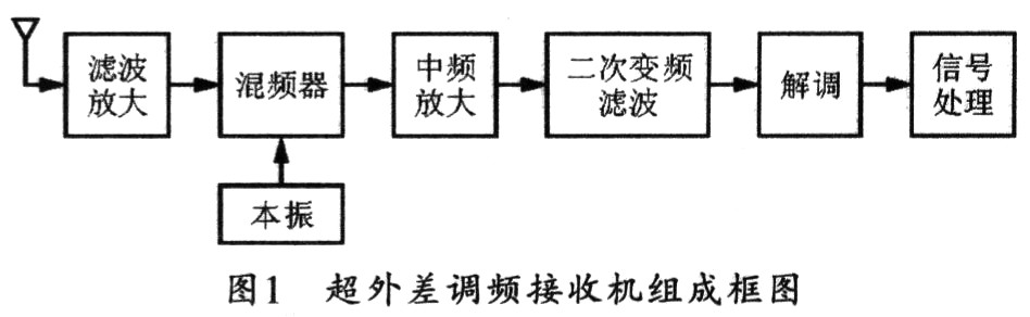
2 Composition of FM receiver Figure 1 shows the basic structure of a typical superheterodyne receiver, namely the composition block diagram of FM receiver. When the antenna receives the high-frequency signal and enters the tuning loop, it is amplified by the RF amplifier stage and then enters the mixing stage. At this time, another high-frequency signal output by the local oscillator also enters the mixing stage, and the output of the mixing stage is a signal containing frequency components such as sum frequency and difference frequency. The output of the mixing stage selects the intermediate frequency signal through the tuning loop, and then is amplified by the intermediate frequency amplifier to obtain a sufficiently high gain, then after the TA31136 is mixed again, and the low frequency signal is demodulated by the frequency discriminator, and finally the low frequency power amplifier Level magnification. Because the high-frequency signal received by the antenna after mixing, it will become a fixed intermediate frequency and then be amplified, so the sensitivity of the receiver is high.
This receiver adopts superheterodyne receiving mode and uses two down conversions. The first intermediate frequency is 21.4 MHz and the second intermediate frequency is 455 kHz. Its receiving channel is 162.025 MHz, the signal bandwidth is 25 kHz, the demodulation method adopts FSK mode, the sensitivity is -110 dBm, and the wireless impedance is 50 Ω.
3 TA31166 IF demodulation chip The most important one in this receiving module is the TA31136 IF demodulation chip, which is the second IF detector. TA31136 is mainly used to perform secondary mixing and demodulate the fundamental frequency signal, and then use the operational amplifier TL062 to level shift the fundamental frequency signal and send it to the communication board for processing.
3. The main characteristic and pin function of TA31166 TA31136 is the bipolar linear integrated chip of Toshiba Company, often used in the frequency modulation IF demodulation of wireless telephone. The chip is packaged in SSOP and has a low operating voltage. The characteristics of TA31136 are as follows:
◇ Low working voltage: Vcc = 1. 8 ~ 5.5 V;
â—‡ Good temperature characteristics;
◇ High sensitivity, 12 dB sensitivity is 11dBuV EMF (input 50Ω);
◇ High intercept point, 96dBuV (input 50Ω);
◇ Built-in 2nd order mixing frequency, working frequency is 10 ~ 100 MHz;
â—‡ Built-in noise detection circuit;
â—‡ With signal strength indication function.
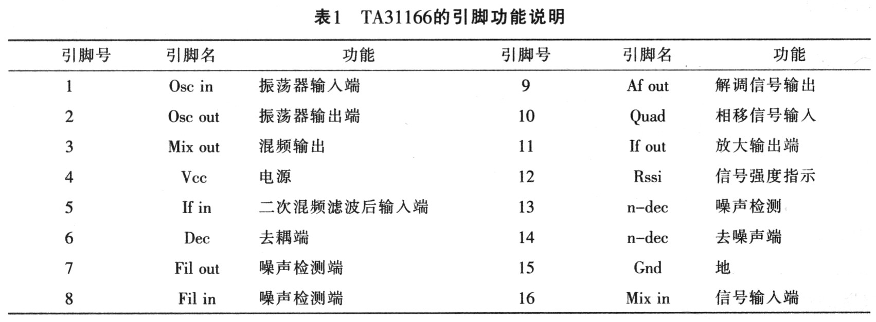
Table 1 lists the pin functions of TA31166.
3.2 Typical application circuit of TA31166 Figure 2 shows the typical application connection diagram of TA31136. The first intermediate frequency signal (21.7 MHz) is filtered through the crystal filter to remove the adjacent clutter signal, and then amplified by the resonant amplifier. Pin 16 is input and internally mixed with the local oscillator signals of Pins 1 and 2 (21.245 MHz) to obtain the second intermediate frequency of the difference frequency of 455 kHz. The output of Pin 3 is filtered by the 455 kHz ceramic filter to remove unwanted signals After input by pin 5, it is amplified by intermediate frequency and then integrated detection, demodulate the audio signal, and output by pin nine. The output signals of TA31136 include inverting amplified output (7 feet), demodulated AF signal output (9 feet), intermediate frequency amplified signal output (11 feet) and so on. Pin 10 is a phase-shifting network, which can be connected to a mid-cycle with a resonance frequency of 455 kHz. TA31136 has high sensitivity and built-in noise detection circuit and RSSI (Received Signal Strength Indication) function, and can output DC level for intermediate frequency amplifier according to input signal level. In order to ensure the same signal size before demodulation under the received signals of different sizes, the circuit also has an automatic gain control (AGC) circuit. The amplification factor during AGC operation is linearly proportional to RSSI. Therefore, by calibrating the AGC The magnification can guarantee the output result of AGC to calibrate the accuracy of RSSI. The voltage of pin 9 of TA31136 is variable. The voltage is 1.11 V at the frequency of the receiving channel. If the frequency is changed, the voltage will drop.
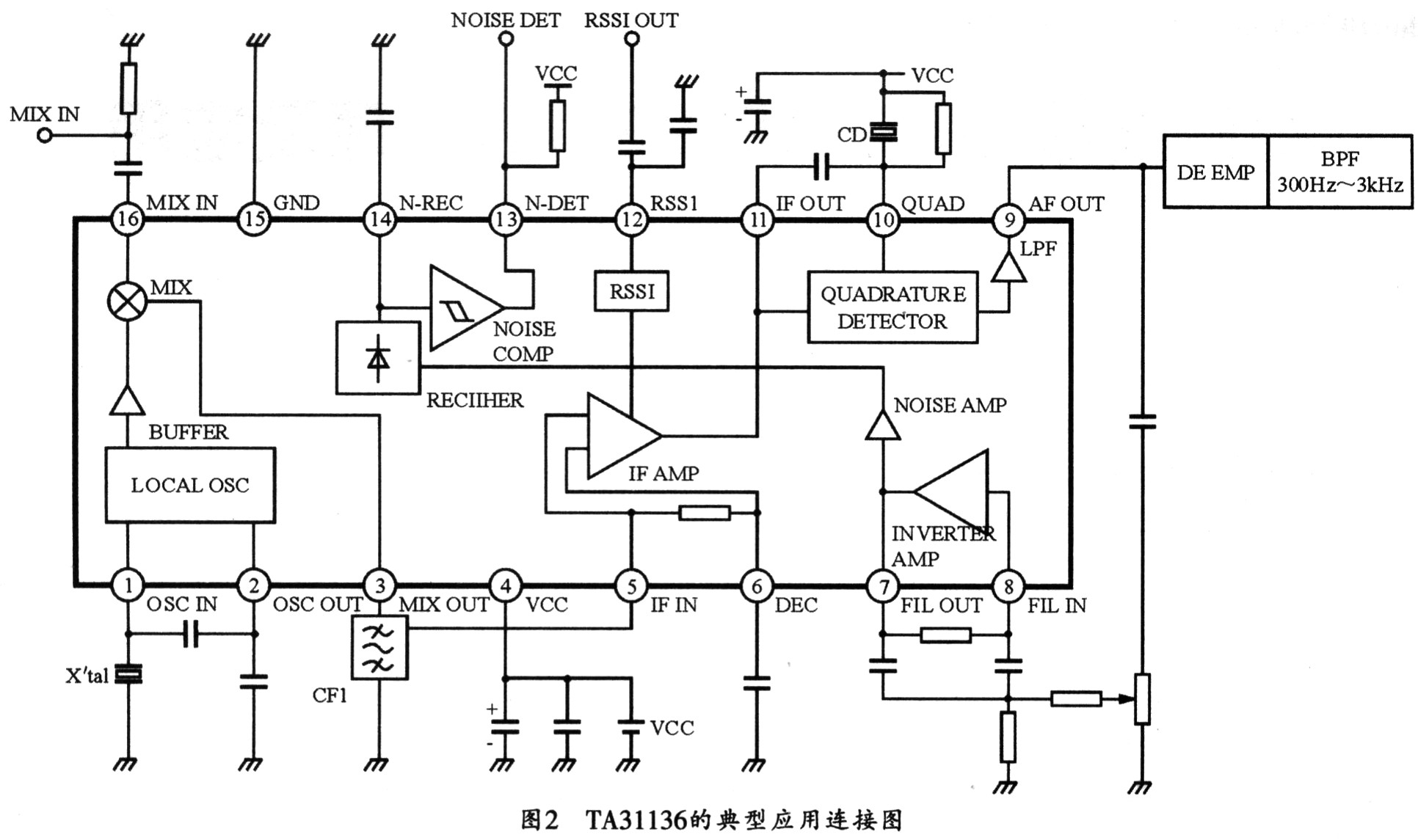
When implementing noise suppression detection, a part of the audio signal output by TA31136 can be divided into resistors 7 and 8 of the intermediate frequency integrated circuit, and the noise component can be amplified and rectified by the internal filter and amplifier of the chip to generate a The DC voltage corresponding to the noise component is sent to the analog port of the MCU for detection. The input DC voltage can be compared with a preset voltage value, and then the output of the speaker can be turned on or off according to the comparison result. In order to ensure that the receiver outputs no noise when there is no input signal, the MCU then outputs the high and low voltage signals according to the comparison result to control the 14 pins of the 31136 to realize the opening and closing of the squelch when receiving the signal. When pin 14 receives a signal, it is 1. 7V high level, when there is no signal, it is 0 V low level.
4 Radio receiving circuit based on TA31136 Figure 3 shows the application circuit diagram of TA31136 in this receiver. The Vcc of this circuit uses 5 V power supply. The received signal becomes 21.7 MHz after the first frequency conversion, and then passes through two 21.7 MHz crystal filters to enhance the selectivity of the input signal. T10 is the middle frequency of the resonance frequency of 21.7 MHz, and a frequency selective amplifier is formed with the transistor Q2. VCC2 is 5 V, which can provide bias voltage to the transistor. U3 (TA31136) mixes the 21.7 MHz signal input at pin 16 with the local oscillator signal at pin 21.245 MHz to form a second intermediate frequency of 455 kHz. After being amplified by the intermediate frequency, the demodulated signal from the middle frequency of the 455 kHz frequency discriminator passes through the low-pass filter composed of the internal resistor R64 and the external capacitor C116. After filtering out the intermediate frequency and higher harmonics, it enters the low amplifier circuit. This program used the mid-week before the frequency discriminating part from the 10th and 11th pins. It was found that the middle-period coil was difficult to debug. Later, the ceramic frequency discriminator CDB450C24 from Murata was used. Because the CDB450C24 has a simple structure and is easy to implement, the frequency is precisely plus or minus 1%, the bandwidth is about 10 kHz, and no load capacitor is required.

5 Conclusion Using the double conversion scheme not only can disperse the total gain of the receiver to three amplification stages of high frequency, intermediate frequency and baseband, but also the local oscillator signal can be more effectively isolated from the received signal. Because the double frequency conversion has one more filtering than the single frequency conversion, the anti-interference ability of the relative clutter is stronger, so it has better anti-interference degree than the single frequency conversion. However, superheterodyne circuits also have shortcomings, and image frequency interference will occur. If the image frequency is located in the pass band of the input loop, the frequency conversion effect of the heterodyne will move the image frequency position and nearby radio signals into the intermediate frequency band, thereby causing interference to the received signal. In order to improve the image frequency suppression capability and sensitivity, and at the same time make the input loop maintain a relatively uniform sensitivity in the entire band, the trap frequency or absorption loop can be used to completely suppress the image frequency during design.
SCSI Connector
SCSI Connector
ATKCONN ELECTRONICS CO., LTD , https://www.atkconn.com