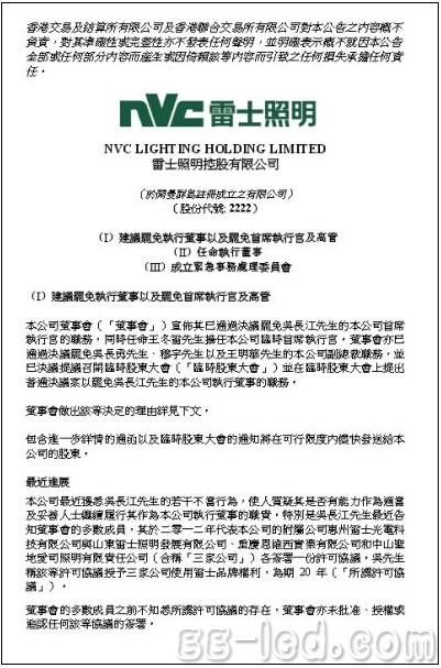
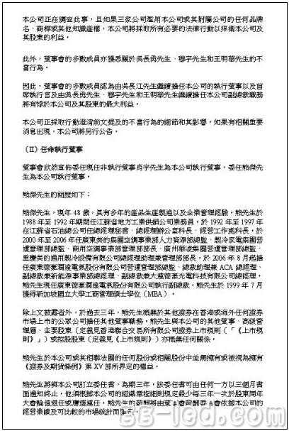
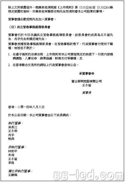
NVC Lighting said in the announcement that the company was recently informed of some of Wu Changjiang’s misconduct. According to the announcement, Wu Changjiang, in the absence of knowledge of most board members, represented Huizhou NVC Optoelectronics Technology Co., Ltd., a subsidiary of the company in 2012, and Shandong NVC Lighting Development Co., Ltd. and Chongqing Enweixi Baoye Co., Ltd. Zhongshan Shengdi Aisi Lighting Co., Ltd. signed a license agreement to grant the above three companies the right to use the NVC brand for a period of 20 years.
NVC Lighting stated that the above agreement has not been approved or authorized by the board of directors.
Also dismissed from Wu Changjiang were the three vice presidents of NVC Lighting, Wu Changyong, Mu Yu and Wang Minghua. Wu Changyong is Wu Changjiang's younger brother, and Mu Yu is also considered to be Wu Liangjiang's right-hand man.
In 1998, Wu Changjiang founded NVC Lighting. In 2010, NVC Lighting was listed on the Hong Kong Stock Exchange. On May 25, 2012, Wu Changjiang resigned from the company's position as chairman, executive director and chief executive officer of NVC, for personal reasons. In June 2013, Wu Changjiang returned to NVC Lighting as an executive director.
In the announcement, NVC Lighting appointed Wang Donglei as CEO and also appointed Xiao Yu and Xiong Jie as executive directors.
Attached: NVC lighting this announcement screenshot
Usually,10 & 20 layers PCB are HDI board,but some are not .Some with big trace width and space,holes are over 0.3mm too. We have much experience in doing 10 Layer PCB & 20 layer PCB.
A ten-layer board should be used when six routing layers are required. Ten-layer boards, therefore, usually have six signal layers and four planes. Having more than six signal layers on a ten-layer board is not recommended. Ten-layers is also the largest number of layers that can usually be conveniently fabricated in a 0.062" thick board. Occasionally you will see a twelve-layer board fabricated as a 0.062" thick board, but the number of fabricators capable of producing it are limited..
High layer count boards (ten +) require thin dielectrics (typically 0.006" or less on a 0.062" thick board) and therefore they automatically have tight coupling between layers. When properly stacked and routed they can meet all of our objectives and will have excellent EMC performance and signal integrity.
A very common and nearly ideal stack-up for a ten-layer board is shown in Figure 12. The reason that this stack-up has such good performance is the tight coupling of the signal and return planes, the shielding of the high-speed signal layers, the existence of multiple ground planes, as well as a tightly coupled power/ground plane pair in the center of the board. High-speed signals normally would be routed on the signal layers buried between planes (layers 3-4 and 7-8 in this case).
10 Layer PCB
10 layer PCB 10 layer TG170 PCB 10 layer design
Storm Circuit Technology Ltd , https://www.stormpcb.com