In the design and use of the SoC system, real-time monitoring of its internal behavior is very important. Currently, it is commonly realized by monitoring information communication between the monitoring terminal and the target system. The UART is often used as a communication channel.
The target SoC system often uses the interrupt mode or the polling mode to obtain the monitoring communication data packet, parses it, and responds with the corresponding data operation. In the interrupt mode, the SoC needs to complete the save interrupt site, call the interrupt service program, and resume the field series task. The context switch occupies the system overhead; in the polling mode, the system periodically checks the device request, and if there is data, the corresponding handler is called. A fixed polling cycle increases the data waiting processing time. When the amount of data is small, frequent queries cause a waste of CPU resources.
Aiming at the above problems, a new monitoring method is proposed to design an FPGA communication system, which serves as a bridge for interaction between SoC and monitoring computer data. It is responsible for completing the online monitoring communication process and ensuring debugging information between the debugged system and the debugging host. The interactive reliability of the command can avoid the target SoC frequently handling communication interruption and improve its control performance. The monitoring function realization mechanism and the design method of the main module of the communication system will be discussed. By comparing the communication time consumption of the embedded CPU in different monitoring methods, the method has certain practical value.
1 system composition
Based on FPGA design, the on-chip communication system is shown in Figure 1. The main components are Modbus parsing module and dual-port RAM memory module. When the host computer issues the monitoring command frame data, the Modbus module completes the process of receiving and parsing the command frame, and stores the information such as the address and data to be operated into the dual-port RAM, and the target CPU accordingly sets the corresponding data of the memory image area thereof. After moving into the dual-port RAM, after the transfer is completed, the Modbus protocol module performs the response data framing and sends back the response data to the monitoring host computer to realize real-time and reliable collection of the monitoring data.
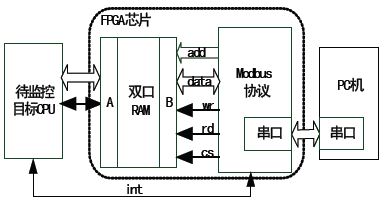
Figure 1 Communication system structure
2 Data interaction design based on dual port RAM
2.1 Dual port RAM customization and memory mapping design
The storage state of the data to be monitored in the target SoC is stored in the memory, which can be abstractly represented as the memory image in FIG. 2.
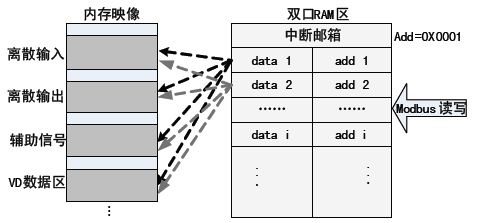
Figure 2 Memory mapping mechanism of dual-port RAM
The dual port RAM stores the current data object to be monitored set, which is a subset of data of the target CPU memory image area. Since the current monitoring object can randomly fall on any storage block in the memory image area, the memory mapping mode of the dual port RAM is selected as a random mapping, as shown in FIG. 2 .
The monitoring objects scattered in the CPU memory image area are mapped to the contiguous storage area in the dual port RAM. When the host computer communicates with the FPGA system on chip based on the Modbus protocol, it accesses consecutive address units to ensure data access speed and improve system communication efficiency.
2.2 Data operation design in dual port RAM
2.2.1 Upper computer reads and writes to dual port RAM
The PC host computer is the communication initiator, connects to the FPGA on-chip system through the serial port, uses the Modbus-RTU protocol for data communication, completes the operations of reading and writing the operating parameters, and realizes the monitoring function.
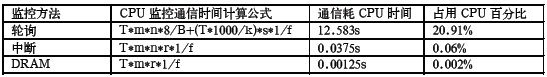
Table 1 Monitors the communication process to take up CPU time
The user inputs the information of the object to be monitored in the man-machine interface, and the background software forms a monitoring command frame according to the Modbus frame structure and the agreed dual-port RAM memory mapping mechanism and sends it through the serial port. The FPGA on-chip system parses the received command frame, obtains the operation function code, the target address, the packet size and other information, and writes the to-be-operated data address set to the dual-port RAM area, and applies for communication to the target CPU after the writing is completed. Interrupted. According to the data operation length given in the Modbus command frame, multiple data units can be read/written at a time.
2.2.2 Target CPU reads and writes to dual port RAM
After receiving the communication interrupt request, the target CPU reads the interrupted mailbox of the dual-port RAM area. The mailbox information includes the function (read or write) of the application and the number of data items requested. According to the application address set, move the corresponding data set of the memory image area into the dual-port RAM once, or move the data set in the dual-port RAM to the corresponding address of the memory image area once. After the move is completed, the interrupted mailbox is cleared, and the interrupt response is sent to the monitoring module. .
[Energy Saving]: Switch it on and it lights up in low light, in the day it automatically turns off whilst the solar panel absorbs the suns energy and charges up its batteries.No longer have to pay for electricity bills or replacing batteries.
[Superior Performance]: This outdoor Solar Light adopt 2020 newly 150mAh solar panel with built-in 800mAh NI-MH battery, each solar lights can light up for up to 8-12 hours after 6-8h full charge.
[Advanced Design]: Equipped with 12 led instead of 8 led to provide brighter light. Full PC lampshade increase irradiation area.High strength ABS Withstand 200KG, don't need to worry about automobile and kids stepping on.
[IP68 Waterproof]:Our disk lights adopt IP68 dust prevention water proofing designs,even the switch is covered with moisture-proof silicone. Zero problems for a raining day.[Easy to Install]: Just press the heavy-duty stakes into the ground, push the button once in the back and it start working forever.No messy wiring or electricity bills needed. Of course you would have to place these solar ground lights where it gets maximum exposure to sunlight.
Solar Pathway Light,Garden Lawn Lights,Solar Lawn Lights,Solar Decoration Light
Ningbo Wason Lighting Technology Co.,Ltd , https://www.wasonlight.com