**1. Open Drain (OD) Output:**
An open-drain (OD) output is very similar to an open-collector output, but instead of a bipolar junction transistor (BJT), it uses a MOSFET. In this configuration, the collector becomes the drain, and the term "open collector" becomes "open drain." The working principle remains largely the same.
In an open-drain setup, the output corresponds to the drain of the MOSFET. To achieve a high logic level, an external pull-up resistor is required. This type of output is ideal for current-driven applications and has a strong ability to sink current—typically up to 20 mA.
To implement a "wire-AND" function, an open-collector (OC) gate is used. It consists of a BJT or MOSFET with matching parameters, and it's typically implemented in a push-pull configuration. Each transistor handles either the positive or negative half-cycle of the signal. During operation, only one of the power switches is conducting at a time, which minimizes conduction loss and improves efficiency. The output can both sink and source current, depending on the circuit design.
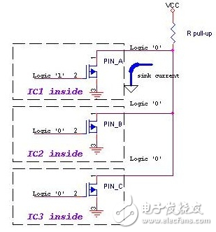
Open drain and open collector concepts are commonly encountered in circuit design. The "drain" in an open drain refers to the drain terminal of a MOSFET, while the "collector" in an open collector refers to the collector of a BJT. An open drain circuit uses the drain of a MOSFET as its output, often with an external pull-up resistor connected to the drain. A complete open drain circuit includes the open drain device and the pull-up resistor, as shown in the figure below:
The characteristics of an open drain circuit include:
1. **Reduced internal drive requirements:** By using the external circuit’s drive capability, the IC’s internal drive is minimized. When the internal MOSFET is on, current flows from the external VCC through the pull-up resistor and into the MOSFET to ground. Only a small gate drive current is needed inside the IC.
2. **Multiple open drain outputs on a single line:** Multiple open drain outputs can be connected to the same line, creating a logical AND function. If any of the pins go low, the entire line goes low. This is the principle behind I2C and SMBus communication protocols. A pull-up resistor must be connected, and when capacitive loads are present, the rising edge is slower due to the passive resistor, while the falling edge is faster due to active driving. High-speed applications may require larger pull-up resistors, increasing power consumption.
3. **Voltage level shifting:** The output high level can be controlled by changing the voltage of the pull-up supply. For example, if the IC operates on Vcc1, the output high level can be set to Vcc2, allowing for level conversion between different voltage domains, such as TTL and CMOS.
4. **Only low-level output without a pull-up resistor:** Without an external pull-up resistor, an open drain pin can only output a low level. This is why the classic 51 microcontroller’s P0 port requires an external pull-up resistor to output a high logic level.
5. **Unidirectional output capability:** Standard open drain pins are designed for output only. Additional circuits can allow for bidirectional operation.
6. **CMOS output stage modification:** In a standard CMOS output, both the upper and lower transistors are present. Removing the upper transistor creates an open drain output. Its main purposes are level shifting and bus line sharing.
7. **Line-AND functionality:** When multiple circuits need to pull down the same signal, open drain is useful. If a circuit does not want to pull low, it will output a high level, which is achieved via an external pull-up resistor. Unlike a standard CMOS output, where a high and low output could cause a short, open drain avoids this issue.
8. **Rising edge delay:** The main drawback of open drain is the delay on the rising edge, caused by the external pull-up resistor charging the load. A smaller resistor reduces delay but increases power consumption. If timing is critical, it's better to use the falling edge.
**Important Application Notes:**
1. **Open collector vs. open drain:** While the principles are similar, open collector is more common in older designs. For example, when driving an input with an open drain, a BJT can be used to create an open collector configuration, which is cost-effective.
2. **Pull-up resistor value:** The value of the pull-up resistor determines the speed of the signal transition. Larger resistors slow down the rise time but reduce power consumption.
**Push-Pull Output:**
A push-pull output is a type of output stage that uses two transistors (one N-type and one P-type) to drive the output. One transistor "pushes" current to the load, while the other "pulls" current from the load. This configuration is widely used in CMOS circuits due to its efficiency and strong drive capability.
Push-pull outputs are suitable for high-current applications and are commonly found in power supplies and amplifier circuits. They offer fast switching, low distortion, and efficient power usage.
However, there are some drawbacks. Push-pull configurations require a center-tapped transformer, and the switch transistors must withstand higher voltages. Additionally, leakage inductance can cause voltage spikes during switching, requiring careful filtering.
**Understanding Push-Pull Output:**
A basic push-pull circuit consists of two complementary transistors—one NPN and one PNP. When one is on, the other is off, ensuring that only one transistor conducts at a time. This prevents short-circuiting and improves efficiency.
For example, when the input voltage is high, the NPN transistor turns on, pushing current to the load. When the input is low, the PNP transistor turns on, pulling current from the load. This results in a clean, full-swing output signal.
**Example of Push-Pull Output:**
In traditional 8051 microcontrollers, the I/O ports can only be used as standard bidirectional interfaces. To drive LEDs, they can either sink current or require an external transistor for amplification. However, in push-pull mode, the I/O can actively drive high levels, making it more versatile.
By connecting LEDs to both I/O lines and setting one as push-pull and the other as a sink, you can control the LED directly without needing separate VCC and GND connections. This method is commonly used in LED dot matrix displays, where rows and columns are controlled based on the desired lighting pattern.
Customized Solar Panel
Customized Solar Panel, 100watt solar panel,200watt solar panel, big solar panel, high efficiency high quality solar modules
different power customized and OEM logo customized solar panel
Customized solar panel data
|
solar cell type
|
mono crystalline half cut cell
|
|
power range
|
50watt to max 700watt
|
|
size and weight
|
different size and different weight if the power is different
|
|
solar panel type
|
monofacial or bifacial
|
|
solar panel color
|
sliver or black
|
Product details and pic


Customized Solar Panel,Noncrystalline Solar Panel Module,Cheap Price Pv Solar Module,Solar Photovoltaic Pv Panel
PLIER(Suzhou) Photovoltaic Technology Co., Ltd. , https://www.pliersolar.com