Most automotive electronic systems require overvoltage, reverse battery, and transient protection. Active protection devices in these protection circuits provide low power, optimum operating voltage thresholds, reduced device cost, and reduced quiescent current. This article discusses in detail the advantages of active solutions over traditional protection circuits.
This article refers to the address: http://
introduction
A wide variety of electronic and electromagnetic interference inside and outside the car often puts the automotive electronics in dangerous working conditions, degrading the performance of the electronic device, and may cause malfunction or even damage. The most severe disturbances—large values ​​of forward, reverse overvoltage, and transient—are mostly caused by internal, or inappropriate (wrong) operation of the automotive electronics system.
Transient voltage generated inside the car
In automotive electronic networks, electronic control units (ECUs) are interconnected by harnesses, and most ECUs are powered by car batteries either directly or through a start switch. Even in normal operation, there are electrical and high-frequency effects that are transmitted through the wiring system, eventually coupling or radiating into the in-vehicle electronic device. Sources of interference include start-up systems, AC motors, load switching, switching jitter, and “load dumping†(ie, the voltage that is turned off during DC motor operation, resulting in voltage).
The most devastating of these surges is the “load throw†(Figure 1), which occurs when the engine is running and disconnects the battery while the AC motor is charging the battery. The magnitude of the transient voltage generated depends on the speed of the AC motor and the amount of field excitation when disconnected. This surge can last for hundreds of milliseconds, producing voltages above 100V, with potentially fatal effects on semiconductor circuits.
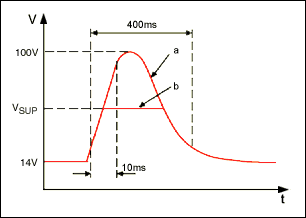
Figure 1. Typical throw load surge waveforms: a) no suppression; b) provide suppression.
Start, cold start, reverse battery
Another risk is the “dual battery†voltage that exists during the startup process. At this point, the cable jumps to the car battery of another group of 24V network systems, and finally the 12V system is turned on with the 24V battery. Let's consider another situation. When starting the engine, especially in cold weather, when the battery is not full, the oil becomes very viscous, the engine needs to provide more torque, so the battery needs to supply more current. Large current loads can cause the supply voltage to drop from the nominal 12V to below 5V. This drop can last for tens of milliseconds, causing the electronic system to hang for a short time (Figure 2). Once the engine is started, the voltage will return to the nominal value.
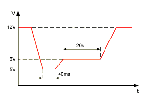
Figure 2. Typical voltage waveform for a cold start of the car
Another noteworthy factor is that when the battery is connected incorrectly, the car electronics must be able to withstand the reverse voltage of the battery (eg -14V).
Protection in case of power failure
The above abnormal conditions prompt the designer to select appropriate protection measures to avoid the effects of power failure. Analysis shows that the load dump pulse is the most energetic type of interference. In order to avoid damage to electronic circuits caused by such pulses, there are currently two protection measures: Central voltage clamping is used inside all automotive AC motors (central load dump suppression, Figure 1b). A protection circuit is provided for each ECU.
The system still requires a second stage of suppression circuitry to filter out low energy pulses on the board, such as positive and negative transient voltages and spikes caused by instantaneous battery reversal. These pulses are typically filtered through small-sized, large-capacitance capacitors, reverse-protected diodes, or inductors in series with a transient suppression diode (TVS) or variable resistor.
Central load dump suppression is typically achieved by an internal alternator's internal clamp circuit (diode) that absorbs the load-dump energy and withstands the battery voltage at startup. Despite the clamping measures, if the clamp voltage is set above the maximum startup voltage, the clamp will not be achieved and the vehicle voltage will still be as high as 36V.
Automotive electronic systems that do not have central load dump suppression must use local protection to suppress load dumping. Usually, away from the connector end, a protection circuit is added inside the ECU, and a large number of such protection measures are required inside the entire automobile, and excessive components may cause leakage current and overall cost increase. On-board load-shedding protection circuits typically use TVS diodes (similar to Zener diodes), variable resistors, and suppression filters. These components should be connected to the power supply.
Various conventional on-board protection circuits are given below.
Standard overvoltage suppression device
There are several types of devices available at the board level for overvoltage clamping.
.
TVS diode
Avalanche diodes (similar to Zener diodes, Figure 3) are capable of suppressing all clamp devices that exceed their breakdown voltage. They absorb higher energy and protect electronic circuits from spikes and load dumps. These diodes feature fast turn-on, slow turn-off characteristics. Avalanche diodes respond faster to overvoltage events than other overvoltage protection devices such as variable resistors. Its performance index will not decrease with the increase of service life and the increase of the number of transient voltage actions. The avalanche suppression diode has a large leakage current near its breakdown voltage. Such diodes are often referred to as Transil®, TransZorb® or simply TVS diodes.
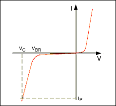
Figure 3. Transient Voltage Suppressor Characteristics (VBR = breakdown voltage, VC = clamp voltage corresponding to peak pulse current IP).
Variable resistor
The variable resistor is a voltage dependent resistor (VDR). Correspondingly, the resistance of the varistor is rapidly reduced after a certain voltage is higher (Figure 4). When clamping positive and negative voltages, it functions like a back-to-back Zener diode. It can withstand relatively high currents and energy with a small package size and low cost, but when the voltage is close to the clamp voltage, the leakage current is large. The clamping voltage also increases significantly with increasing current. Variable resistors can be affected by repeated surges and often have higher "clamping voltages" that significantly reduce their response speed compared to TVS diodes.
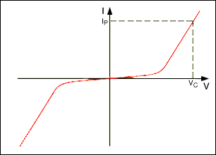
Figure 4. Typical Variable Resistor Characteristics (VC = Clamping Voltage for Peak Pulse Current IP)
Discrete protection circuit
A simple and cost-effective protection circuit is to connect the load in parallel with a clamp circuit (such as a TVS diode) and add a fuse before the capacitor (Figure 5). This circuit allows the ECU to protect the system from transient overvoltages and load dump conditions above the TVS diode (D1) breakdown voltage. When a negative transient voltage or a stable reverse voltage occurs, the TVS is forward-conducting, clamping the negative voltage to its turn-on voltage (eg, -1V) to provide protection for subsequent circuits. For lower energy negative transient voltages, such as those introduced by relays or solenoid switches, they can be filtered out by a capacitor (ClowE). If the forward or reverse overvoltage condition is maintained, the fuse will blow.
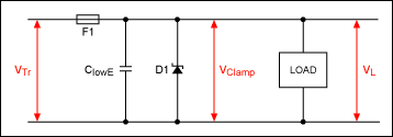
Figure 5. Simple overvoltage protection circuit with filter capacitor, transient suppression diode, and fuse
In order to avoid replacing the fuse at the inaccessible ECU or to ensure continuous operation of the ECU, other techniques must be employed, such as additional series protection. The circuit of Figure 6 protects the ECU from reverse voltage and transient undervoltage (D2), forward overvoltage pulses (load dump and low energy transient voltage) above the TVS diode (D1) breakdown voltage. The reverse peak voltage of the selected diode D2 must be greater than the maximum negative pulse that may occur.
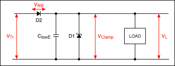
Figure 6. Replace the fuse in Figure 5 with a diode that provides overvoltage protection and provides negative transient voltage protection and reverse battery protection.
.
Considering its small size, low cost, and high power dissipation capability, variable resistors are often used in systems where board area requirements are critical and subsequent circuits have some tolerance to forward and reverse overvoltages. The circuit shown in Figure 7 provides effective overvoltage pulse protection (positive and negative transient voltages above the breakdown voltage of the variable resistor) for subsequent circuits. Capacitors help to filter out low-energy positive and negative transients.
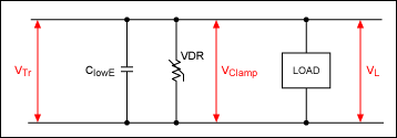
Figure 7. When the board area is limited and the overvoltage protection needs to be provided for subsequent circuits, the variable resistor (VDR in the example) can be used instead of the TVS diode as long as the overvoltage pulse (positive or negative transient pulse) is high. For the breakdown voltage of the variable resistor, when a positive or negative overvoltage occurs, the subsequent circuit must have a certain capacity.
Advantages and disadvantages of discrete protection circuits
All of the above circuits have their own advantages and disadvantages. The circuit shown in Figure 5 is a simple transient protection circuit that contains only one TVS tube, one filter capacitor and one fuse, but the disadvantage is that the breakdown voltage must be chosen to be greater than the maximum possible stability. State-of-the-art TVS diodes, which are typically twice the battery voltage at startup (often > 26V for more than 1 minute). Otherwise, if the TVS is not properly selected, the TVS tube conducts at a lower voltage and then burns out due to continuous power dissipation.
Since the VI characteristic has limited the slope of the current change above the breakdown voltage, the TVS diode also has a certain internal resistance, which causes the clamp voltage to rise due to the higher current. For example, a 28V TVS tube (such as SMBJ28) will cause the voltage of the subsequent circuit to reach 45V when a load dump occurs. In this case, the subsequent circuit must be able to withstand 45V (Figure 3). Obviously, this will complicate the selection of subsequent ECU circuit components, which typically only operate at the upper limit of the vehicle's nominal operating voltage (approximately 17V). High-voltage semiconductor devices or other components are expensive, increasing the cost of the ECU and taking up valuable board space.
In order to minimize the maximum overvoltage value, it is necessary to select a TVS tube whose breakdown voltage is close to the steady state maximum voltage (for example, the startup voltage). This may cause a large leakage current to occur when the breakdown voltage is approached (even at a nominal 12V vehicle voltage). This leakage current makes it difficult for ECU designers to meet the low quiescent current requirements of OEMs (equipment manufacturers) when the car engine is down.
Under normal operating conditions, the diode (D1) in Figure 6 shows a voltage drop of > 0.7V, which creates two problems: The voltage drop produces a certain amount of power. The ECU is difficult to work in a low pressure state.
For high current applications, such as automotive anti-lock braking systems, the current consumed can easily exceed 10A. For example, a diode with a 1V drop in the system would cause 10W of power dissipation, and dissipating such a large amount of power on a limited-sized board is almost impossible. The use of single or dual Schottky diodes can alleviate this problem in some applications. Assuming a voltage drop of 0.5V, the dual Schottky diode consumes 5W at 10A load current. This is still an unacceptable power consumption, and designers have to use large-size heat sinks.
As mentioned above, the diode drop itself has a certain negative impact. For example, in a 14.4V audio system, the maximum output power depends on the maximum speaker drive voltage that can be achieved. In order to avoid reverse battery connection, a diode is added to the power supply in the system, which may cause a voltage drop of 1V, resulting in an output power loss of about 8.4dBW (for a 2Ω bridge speaker).
When the car is started in a cold environment, the ECU must be able to operate in a low voltage state (Figure 2). Any unnecessary voltage drop will affect the system operation. At cold start, the car manufacturer specifies an input voltage of 5.5V or less. The diode drop used to prevent reverse battery connection can take up a lot of headroom. For example, the car battery voltage drops to 5.5V at the ECU input connector, minus the 0.7V voltage drop across the battery reverse-connected protection diode, and the voltage actually supplied to the circuit is only 4.8V.
If the 5V microcontroller is powered by a linear regulator with a differential voltage of 500mV, the microcontroller can obtain a supply voltage of only 4.3V, which cannot support its normal operation, and may cause it to enter the reset state and lose memory data. Or cause the entire ECU to crash. The GPS navigation system is a typical example: the car enters the destination address before starting, and the system must ensure that no data is lost during the cold start.
For the application of the variable resistor shown in Figure 7, the board area is usually very strict. As with the TVS tube, the clamp voltage of the variable resistor is determined based on the highest steady state DC voltage for the particular application. However, when the voltage is higher than the breakdown voltage, the VI characteristic curve of the variable resistor is much slower than that of the TVS diode (Fig. 4). Therefore, the variable resistors withstand the higher voltage of the subsequent circuit relative to the TVS tube, thereby increasing the device cost, package size, and board space of subsequent circuits.
By setting the clamp voltage at a relatively low level, keeping the overvoltage protection point as low as possible increases the quiescent current during normal operation. The quiescent current at the nominal voltage is usually higher than the TVS tube, and the actual effect is related to the specific component selection.
Active transient protection scheme
Considering the many shortcomings of the above discrete protection circuits, the active protection circuit provides a better choice. For solutions that require low quiescent current, low operating voltage, and reverse battery protection and overvoltage protection, the MAX16013/MAX160141 overvoltage protection/detection circuit can be selected.
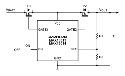
The working principle of such devices is very simple (Figure 8). The IC directly monitors the input voltage and disconnects the load under fault conditions by controlling two external pFET power switches. The external MOSFET is turned on between 5.5V and the set upper supply voltage. The upper limit voltage can be adjusted by a voltage divider resistor connected to the SET pin, typically between 20V and 28V.
.
Figure 8. The MAX16013 and MAX16014 provide active transient protection to directly monitor the supply voltage and, when a fault is detected, disconnect the load and fault supply by controlling two external p-channel FET switches.
In the event of a fault, FET P2 has two different modes. In the first mode, P2 is only equivalent to a simple switch that opens the switch under overvoltage conditions, thereby avoiding high voltage damage to downstream components. In the second mode, P2 is equivalent to an adjustable transient suppressor that clamps the output voltage to the maximum allowable overvoltage point.
When the output voltage rises above the adjustable overvoltage threshold, the internal comparator pulls GATE2 up to VCC. When the monitored voltage drops below the overvoltage threshold, the p-channel MOSFET (P2) turns back on. This type of processing stabilizes the voltage within 5% of the output regulation. The output is stable when a transient overvoltage occurs. The MOSFET (P2) remains on under overvoltage conditions and operates in a switch-linear regulation mode to provide overvoltage protection while maintaining system operation.
Connect the voltage divider resistor of the SET pin to the input or output to select the appropriate operating mode. For example, to connect a voltage divider resistor to VCC (instead of a load), the MAX16013 is configured to overvoltage shut down the device. The MAX16014 will keep the MOSFET (P2) latched until the input supply is powered back on or the EN is re-triggered. If the MAX16013 is operating in voltage-limiting mode for an extended period of time, the voltage drop across the external MOSFET increases power dissipation.
The battery reverse protection FET (P1, optional) in Figure 8 replaces the series diode in Figure 6. In Fig. 8, P1 is turned on during forward bias, which can maintain a very low forward voltage drop and turn off when a negative voltage occurs. Turning off P2 disconnects the input and output (Figures 8 and 9), and the EN pin provides the appropriate shutdown control (note that the control signal for the EN pin is generated by the other supervisory circuits of the host system). Therefore, when the circuit is in reverse battery protection (P1), the quiescent current of the downstream circuit can be minimized (typically < 20μA).
Advantages of Active High Voltage Transient Protectors over Traditional Protection Solutions
Active overvoltage protectors have several advantages.
As mentioned above, the breakdown voltage of a discrete transient suppressor (TVS tube or variable resistor) needs to be higher than the highest steady-state operating voltage of the vehicle (usually around 26V). In the event of a load dump, due to the internal resistance of the TVS tube and the VI characteristic curve of the current surge with voltage, the downstream circuit will withstand extremely high voltage (about 45V) in an instant, thereby increasing the voltage rating of the downstream device. Unlike traditional solutions, active transient protectors clamp the output voltage to the level set by the divider resistor (eg, 26V), and there is no current surge with voltage. These features allow users to use low cost (low voltage) downstream components.
This solution is different from ordinary surge suppressors. The traditional solution can only handle a few joules of energy in a short time before overheating, and the MAX16013/MAX16014-based solution protects the device from DC overvoltage. Some applications require operation at the upper limit of the nominal voltage. Once the upper voltage is exceeded, the connection to the power supply is disconnected (in the case of an audio system, the upper operating voltage is typically 17V). In this case, an active protection device is used, and the threshold of the voltage limiter/switch can be reasonably set to further reduce the cost of downstream components.
By replacing the battery reverse diode with a FET, the forward conduction voltage can be reduced to the millivolt level. Especially in high-current applications, this measure can effectively reduce power consumption, thereby reducing the design difficulty and cost of heat dissipation. The power (voltage) consumed by the original diode can be supplied to the load (eg, the speaker) instead of being consumed on the diode, thereby increasing the output power (system performance). Some applications require a lower battery voltage (eg, when the car is cold-started) and also require reverse battery protection. Active protection devices minimize voltage drop and ensure that the circuit operates at a lower input voltage.
Variable resistors tend to exhibit relatively high quiescent currents and leakage currents, which can significantly affect their lifetime and accuracy when impacted by a pulsed voltage. Replacing a variable resistor with an active protection device can solve this problem. Since the variable resistor is directly connected to the battery in some applications, the leakage current is large. At this point, the active protection device can be used as the main switch to disconnect (via the P2 FET) all subsequent loads in sleep mode (Figure 9).
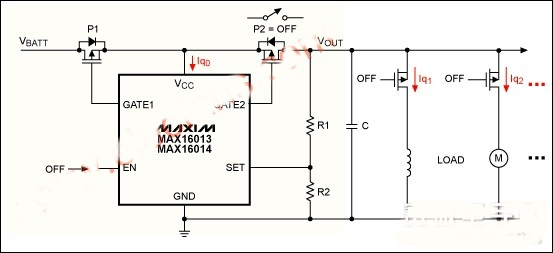
Figure 9. The MAX16013/MAX16014 are used as main switch controls to help reduce quiescent current losses when the ECU is turned off.
to sum up
Active overvoltage protectors have certain advantages in many applications. These devices can significantly reduce system power consumption, increase output power (improve system performance), reduce system operating voltage (cold start), and have lower quiescent current. , reducing the rated voltage requirements for subsequent protected circuits.
UVC Lamp 253.7nm, different type. quartz material .
Uvc Lamp,Uv Germicidal Bulb,Uv Germicidal Lamp,Uvc Tube
Changxing leboom lighting product CO.Ltd. , https://www.leboomuv.com