 A rational interpretation of the superconducting resistance prompted the United States Department of Energy (DOE) affiliate Brookhaven National Laboratory to create a perfect atomic-scale ultrathin film that accurately demonstrated the transition from an insulator to a superconductor.
 Researchers use ordinary insulating copper oxides (cuprates) to form a channel similar to a field effect transistor (FET) while using molecular beam epitaxy (MBE) to grow a perfect atomic-scale superconducting thin film. So far, researchers have demonstrated that the superconducting on-temperature of a material can be adjusted to as much as 30K by applying an electric field, which is more than 10 times higher than previously reported results. Ivan Bozovic, the project's director of research, said.
Bozovic said that their millimeter-scale material also makes it one of the few examples of the performance of quantum mechanical properties in macroscopic samples. His research team also found evidence that Cooper electrons are necessary for superconductivity—a transitional stage before they are actually transformed into superconductors—and that their thin films show precise resistance values. The resistance of superconductors has been predicted by quantum mechanics, which is 6.45KΩ(h/2e2).
Bozovic said that as we continue to explore these mysteries, we are also working hard to make ultra-high-speed energy-saving superconducting electrons possible.
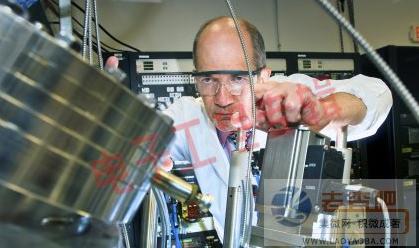
Figure: Ivan Bozovic, physicist at the Brookhaven National Laboratory, wonders why thin-film insulator transitions to superconducting superconducting field-effect transistors will be faster, consume less power, and be packaged more densely than current conventional transistors. , as well as having a new mode of operation such as the ability to adjust superconductivity using an applied electric field.
Bozovic said that this is only the beginning.
Anyang Kayo Amorphous Technology Co.,Ltd is located on the ancient city-Anyang. It was founded in 2011 that specializes in producing the magnetic ring of amorphous nanocrystalline and pays attention to scientific research highly,matches manufacture correspondingly and sets the design,development,production and sale in a body.Our major product is the magnetic ring of amorphous nanocrystalline and current transformer which is applied to the communication, home appliances, electric power, automobile and new energy extensively. We are highly praised by our customers for our good quality,high efficiency,excellent scheme,low cost and perfect sale service.
Fe-based nano-crystalline Ribbon is made of Fe,Si,B,Nb,Cu and so on which is high permeability,high saturation magnetic induction,low loss,high toughness,good wear and corrosion resistance and excellent stability.It can replace the silicon steel,permalloy and ferrite and be used to medium and High Frequency Transformer, mutual inductor and most electronic parts.Especially it is the most cost-efficent in all amorphous ribbons.
Nano Ribbon,Fe-Based Nano-Crystalline Ribbon,Cost -Optimal Ribbon,Best Nano-Crystalline Ribbon
Anyang Kayo Amorphous Technology Co.,Ltd. , https://www.kayoamotech.com