The S (scattering) parameter is used to characterize an electrical network that uses a matched impedance. The scattering here is the way in which the current or voltage is affected in the event of a transmission line interruption. use. The S-parameter can treat a device as a "black box" with inputs and corresponding outputs, so that system modeling can be performed without having to worry about the intricate details of its actual structure.
The bandwidth of today's integrated circuits continues to increase, so performance must be characterized over a wide frequency range. Traditional low frequency parameters, such as resistance, capacitance, and gain, may be frequency dependent, so the performance of the IC at the target frequency may not be fully described. In addition, it may not be possible to characterize each parameter of a complex IC over the entire frequency range, while system-level characterization using S-parameters can provide better data.
A simple RF relay can be used to demonstrate high frequency model verification techniques. As shown in Figure 1, the RF relay can be thought of as a three-port device: an input port, an output port, and a control port for the switching circuit. If the device performance is independent of the control side, once set, the relay can be simplified to a dual port device. Therefore, the device can be fully characterized by observing the behavior of the input and output.
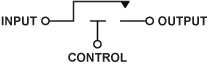
Figure 1. RF relay model
To understand the concept of S-parameters, some transmission line theory must be known. Similar to the well-known DC theory, at high frequencies, the maximum transmission power is related to the impedance of the power supply and the impedance of the load. The voltage, current, and power from a source of impedance ZS travel along a transmission line of impedance Z0 to the load of impedance ZL. If ZL = Z0, then all power is transferred from the power supply to the load. If ZL ≠Z0, some power is reflected back from the load to the power supply and no maximum power transfer occurs. The relationship between the incident wave and the reflected wave is represented by the reflection coefficient Γ, which is a complex number containing information about the amplitude and phase of the signal.
If Z0 and ZL match exactly, no reflection will occur, Γ = 0. If ZL i is open or shorted, Γ = 1, indicating no match, all power is reflected back to ZS. In most passive systems, ZL is not exactly equal to Z0, so 0 “ Γ “1. For Γ to be greater than 1, the system must include a gain component, but the RF relay example will not consider this. The reflection coefficient can be expressed as a function of the correlation impedance, so Γ can be calculated by:

(1)→

(2)
Assume that the transmission line is a two-port network, as shown in Figure 2. In this representation, it can be seen that each traveling wave consists of two parts. From the output of the dual port device to the total traveling wave portion of the load, b2, is actually composed of a portion a2 reflected from the output of the dual port device and a portion a1 of the transmissive device. Conversely, the total traveling wave b1 flowing back to the power supply from the input of the device is composed of a portion a1 reflected from the input terminal and a portion a2 of the returning device.
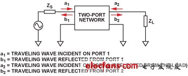
Figure 2. S-parameter model
According to the above description, the formula for determining the reflected wave value can be listed using the S parameter. The calculation formulas of the reflected wave and the emitted wave are as shown in Equations 3 and 4, respectively.
(3)
(4)
If ZS = Z0 (impedance of the dual port input), no reflection will occur, a1 = 0. If ZL = Z0 (impedance of the dual port output), no reflection will occur, a2 = 0. Therefore, we can match The condition defines the S parameter as follows:

(5)

(6)

(7)

(8)
among them:
S11 = input reflection coefficient
S12 = reverse transmission coefficient
S21 = forward transmission coefficient
S22 = back reflection coefficient
These two-port systems can be fully described by these formulas. The forward and reverse gains are characterized by S21 and S12, respectively, and the forward and reverse reflected powers are characterized by S11 and S22, respectively.
To solve the above parameters in the actual system, ZS, Z0, and ZL must match. For most systems, this is easy to implement over a wide frequency range.
When the semiconductor diode is turned on, it is equivalent to the switch closing (circuit is turned on), and when it is turned off, it is equivalent to the switch opening (circuit cut), so the diode can be used for switching, and the commonly used model is 1N4148. Since the semiconductor diode has a unidirectional conduction characteristic, the PN junction is turned on under a positive bias, and the resistance in the on state is small, about several tens to several hundreds of ohms; in the reverse bias, it is off. The resistance is very large. Generally, the silicon diode is above 10 Μ Ω, and the bismuth tube is also several tens of kilo ohms to several hundred kilo ohms. With this feature, the diode will act as a control for the current to turn on or off in the circuit, making it an ideal electronic switch.
Switching Diode,1N4148 Signal Diode,4148 Diode,1N4148 Diode
Dongguan Agertech Technology Co., Ltd. , https://www.agertechcomponents.com