As stated by Moore's Law, the density and performance of integrated circuits have grown rapidly over the decades. As we all know, this trend of rapid growth will one day end, people just do not know the extent to which the density and performance of integrated circuits can reach when this moment comes. With the development of technology, the density of integrated circuits is increasing, and the width of gate oxide is decreasing. The multiple effects commonly found in very large scale integrated circuits become more important and difficult to control. The antenna effect is one of them. In the past two decades, semiconductor technology has grown rapidly, resulting in products with smaller specifications, higher package density, higher speed circuits, and lower power consumption. This article will discuss antenna effects and solutions to reduce antenna effects.
This article refers to the address: http://
Antenna effect
Antenna effect or plasma-induced gate oxide damage refers to an effect that can potentially affect product yield and reliability during MOS integrated circuit production.
Currently, lithographic processes use integrated plasma etching (or "dry etching") to fabricate integrated circuits. Plasma is an ionized/active gas used for etching. It provides super mode control (sharp edge/less undercut) and a variety of chemical reactions that are not possible with conventional etching. But everything has two sides, it also brings some side effects, one of which is charging damage.
Plasma charging damage refers to the unintended high field stress of the gate oxide produced in the MOSFET during plasma processing. During plasma etching, a large amount of charge accumulates on the polysilicon and metal surfaces. Through capacitive coupling, a large electric field is formed in the gate oxide, resulting in stresses that can damage the oxide layer and change the device threshold voltage (VT). As shown in the figure below, the accumulated static charge is transferred to the gate and neutralized by the current tunnel through the gate oxide.
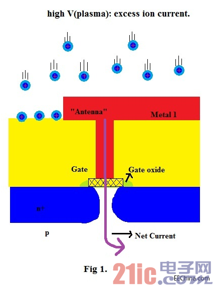
Figure 1: Antenna effects during plasma etching.
It is obvious that the area of ​​the conductor exposed to the plasma is very important, which determines the static charge accumulation rate and the tunneling current. This is the so-called "antenna effect." The area ratio of the conductor under the gate to the oxide layer is the antenna ratio. In general, the antenna ratio can be thought of as a current multiplier that amplifies the density of the gate oxide tunneling current. For a given antenna ratio, the higher the equal particle density, the greater the tunneling current. Higher tunneling current means higher damage.
3 plasma manufacturing processes
Conductor layer mode etching process - The cumulative charge is proportional to the circumference.
Ashing process - The amount of accumulated charge is proportional to the area.
Contact Etching Process - The amount of accumulated charge is proportional to the area of ​​the pass region.
The conventional definition of the antenna ratio (AR) refers to the ratio of the area of ​​the "antenna" conductor to the area of ​​the gate oxide layer to which it is connected. Conventional theory holds that the degree of reduction in antenna effect is proportional to the antenna ratio (the charging effect of each metal layer is the same). However, it has been found that the antenna ratio does not depend on the antenna effect, and layout issues need to be considered.
The effect of layout on charging damage
The degree of charging damage is a geometric function associated with a very dense grid antenna. However, due to the difference in etch rate, etch delay, plasma ashing and oxidative deposition, and plasma induced damage (PID), charge damage is more susceptible to electronic shielding effects.
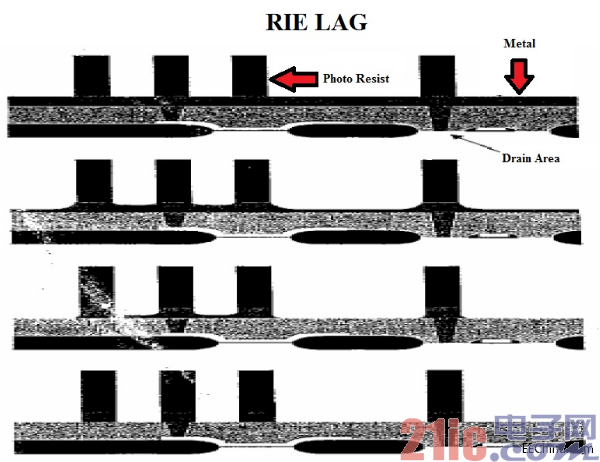
Figure 2: Effect of layout on charging damage.
Therefore, the new mode of antenna effect needs to consider the etch time factor, as in Equation 1. By controlling the antenna effect by inserting a diode or bridge (wiring), the antenna effect can be better predicted, as shown in Equation 2.
Where Q refers to the total accumulated charge injected into the gate oxide during the etching.
A is the area of ​​the conductive layer, and the capacitance capacity under the plasma current density J is C.
a is the gate area, and the capacitance capacity under the plasma current density J is a
为 is the capacitance ratio
P is the perimeter of the antenna capacitor
p is the perimeter of the gate capacitor
ω is the angular frequency of the plasma power supply
According to the new PID-based mode, the PID does not depend on the AR, but the ratio of the antenna capacitance to the gate capacitance is a good indicator of the PID. The PID depends on the frequency of the plasma source. When the oxide layer is <4 nm, the PID will become insensitive to the stress current. By increasing the dielectric constant of the gate without increasing J, the PID can be increased.
Design solutions to reduce antenna effects
The following solutions can be used to reduce the antenna effect.
1. Jumper method: By inserting a jumper, disconnect the antenna with antenna effect and route it to the upper metal layer; until the last metal layer is etched, all the etched metal is connected to the gate.
2. Virtual Transistors: Adding additional gates reduces the capacitance ratio; PFETs are more sensitive than NFETs; problems with reverse antenna effects.
3. Add an embedded protection diode: Connect the reverse-biased diode to the gate in the transistor (the diode does not affect the function during normal operation of the circuit).
4. After layout and routing, insert the diode: connect the diode only to the metal layer that is affected by the antenna effect
A diode protects all input ports connected to the same output port.
The two most important ways to eliminate the antenna effect are the jumper method and the insertion of a diode. Next, we will discuss these two methods in detail. The jumper method is the most effective way to deal with antenna effects. Inserting a diode solves other antenna problems.
Jumper method
The jumper is to disconnect the metal layer with the antenna effect, connect to other metal layers through the via, and finally return to the current layer. As shown in the figure below, the jumper method divides the long antenna into short antennas, reducing the area of ​​the wires connected to the gate input, thereby reducing the accumulated charge.
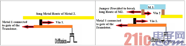
Figure 3: Schematic diagram of the jumper method to reduce antenna effects.
It should be noted that the placement of the jumpers is very important. The jumper must be placed in a position that reduces the length of the wiring. The figure below can be explained in detail. As shown in the figure below, in the two pictures, the input and output pins have the same length of spacing, but the jumper position is slightly different. The circuit in the first picture is not affected by the antenna effect, while the circuit in the second picture is affected by the antenna effect.
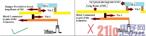
Figure 4: Insert a jumper around the gate.
It can be clearly seen from this example that jumpers (also called "bridges" can be used to avoid antenna effects. The jumper disconnects the metal layer with the antenna effect, passes the static charge through the via to the higher metal layer, and then back to the current layer. In the metallization process, in addition to the highest level, the pins are connected to a small wire area to avoid any antenna problems below this layer.
Insert diode
As shown, inserting a diode next to the logic gate input pin provides a charge bleed path for the underlying circuitry, so the accumulated charge does not pose a threat to the transistor gate. The use of a diode provides a charge bleed path for additional ions that are concentrated on the metal layer by the substrate.
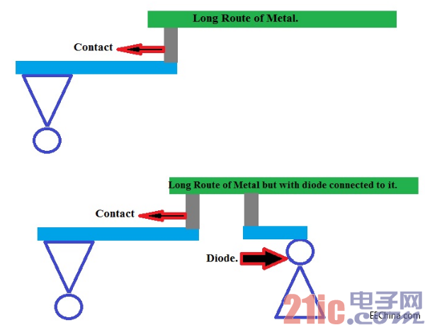
Figure 5: Insert a diode around the logic gate input.
However, inserting a diode increases the input load of the logic gate, which increases the circuit cell area and affects timing. In addition, places where space is small are not suitable for insertion of diodes.

Figure 6: Control antenna effects by inserting diodes or bridges (wiring).
to sum up
During the fabrication of an integrated circuit, a large amount of electrostatic charge is accumulated on the surface due to the exposure of the metal layer. The amount of charge depends on many reasons. From the perspective of the antenna, the amount of charge depends on the exposed area of ​​the metal. The larger the area exposed by the metal, the more charge is accumulated. The substrate is at the bottom and is connected to the fabrication device, thus creating a voltage gradient in the gate oxide. When this gradient becomes large enough, it will be released by an explosive discharge (ie "lightning"). This problem has a very large impact on the small technology field, because the damage caused by the leakage is likely to affect the entire grid.
Since the method of expressing the antenna ratio is not uniform, the antenna rule check is different for each processing technique.
A reverse biased diode can be placed next to the gate that needs to be protected to protect the circuit from antenna effects. The reverse biased diode prevents electrons from flowing between the circuit and the diode during normal operation of the chip and prevents electrons from flowing to the chip substrate. However, during the remanufacturing process, the charge on the circuit will accumulate at a point where the voltage will exceed its tolerance. The voltage at this point is higher than the normal operating voltage of the circuit, but lower than the expected electrostatic discharge voltage in the gate. When this happens, the diode allows electrons to flow from the circuit to the substrate, thus mitigating the charge accumulated in the circuit. This is a non-destructive process and the circuit can be discharged multiple times through the diode during the manufacturing process.
Another way to avoid antenna effects is to "cut" the antenna (ie, "jumper") by changing the metal layer. When the metal layer is formed, a large metal layer on one side is no longer electrically connected to the gate, and thus no antenna effect is generated. When connected by a higher-grade metal "bridge", the conductor surface is no longer exposed and therefore does not collect free charge, thereby avoiding antenna effects.
Wire Feeding Roller is part of the spraying system.
Wire Feeding Roller
Wire Feeding Roller,Welding Wire Feed Roller,Wire Feeder Roller,Wire Feed Drive Roller
Shaoxing Tianlong Tin Materials Co.,Ltd. , https://www.tianlongspray.com