For electronic products, the protection circuit is to prevent the key sensitive devices in the circuit from being damaged by overcurrent, overvoltage, overheating and other impacts. The quality of the protection circuit is critical to the quality and longevity of the electronic product. As demand for consumer electronics continues to grow, stronger electrostatic discharge (ESD) protection is required while reducing unnecessary electromagnetic interference (EMI) / radio frequency interference (RFI) noise. In addition, consumers hope that the latest consumer electronics products can meet increasingly higher download and bandwidth capabilities with smaller devices. As devices become smaller and more immersive, ESD and EMI/RFI suppression in many cases are no longer covered by the next-generation ICs that drive the required interfaces.
In addition, advanced system-on-chip (SoC) designs are fabricated using a small geometry process. To optimize functionality and chip size, IC designers have been continually reducing the minimum size of their designed features. The shrinking IC size makes the device more susceptible to ESD voltage damage.
In the past, it was sufficient for designers to select a protection product that complies with the IEC61000-4-2 specification. Therefore, most data sheets for protected products only include compliance with rating requirements. As integrated circuits become more sensitive, newer designs have protection components to meet standard ratings, but ESD strikes still create excessive voltages that can damage the IC. Therefore, designers must select one or more protection products that not only meet ESD pulse requirements, but also clamp the ESD shock to a low enough voltage to ensure IC protection.
This article refers to the address: http://
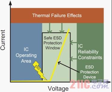
Figure 1: ESD Protection Requirements for the American Electrostatic Discharge Association (ESDA)
Advanced Technology for Powerful ESD Protection The ESD clamp performance of ON Semiconductor is highly regarded by the industry, and the clamping performance can be observed and quantified in several ways. The ESD clamping capabilities of independent ESD protection devices or integrated devices, including ESD protection, can be measured using several standard tools. The first tool is the ESD IEC61000-4-2 ESD impulse response screenshot, showing the clamp voltage response over time, showing the downstream device in the ESD event.
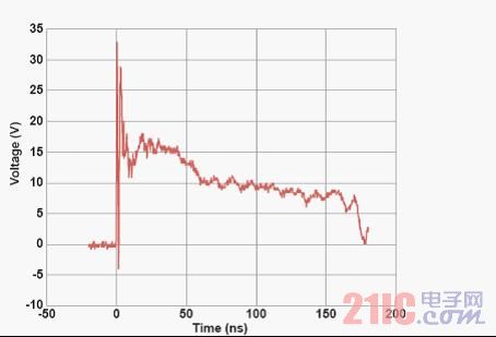
Figure 2: ESD Clamp Clamp Screenshot
In addition to the ESD clamp screen shot, another method is to measure the transmission line pulse (TLP) to evaluate the ESD clamp performance. Since the ESD event is a very short transient pulse, the TLP can measure current and voltage (IV) data, where each data point is obtained from a short square pulse. TLP IV curves and parameters can be used to compare the properties of different TVS devices and can also be used to predict the ESD clamp performance of a circuit.

Figure 3: Typical TLP IV graph
There are two types of high-speed interface ESD protection devices available from ON Semiconductor. The first category is the easiest to implement and is called traditional design protection. In this type of design, the signal line runs under the device. These devices are usually the lowest capacitance products.
The other is a product that uses PicoGuard® XS technology. This type of design uses an Impedance Matched circuit that guarantees 100 Ω impedance, which is equivalent to zero capacitance. This type of design eliminates the need for shunt inductors and helps minimize ESD voltage spikes caused by the package.
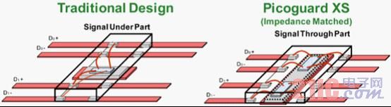
Figure 4: Comparison of traditional methods with PicoGuard® XS design methods
ON Semiconductor's protection and filtering solutions are based on traditional silicon process technology. In contrast, other types of low-cost passive solutions use materials that combine ceramic, ferrite, and multi-layer varistor (MLV). Such devices typically have poor ESD clamping performance. In some cases, the energy delivered to downstream devices may be an order of magnitude lower than the ON Semiconductor solution. Some products with old technology may even deteriorate and become worse after a small amount of ESD shock. Due to their material properties, some passive devices often exhibit temperature inconsistencies, which reduces the reliability of the end system operating over standard consumption temperatures and ambient temperature ranges.
Must take into account other characteristics
ESD and EMI solutions prevent unwanted signals from interfering with the overall performance of the system. The protection device must also maintain good signal integrity for a given interface during normal system operation, in other words it should be completely "transparent". ON Semiconductor's devices are designed to operate and protect today's most popular consumer electronic system interfaces. In general, the S-parameter insertion loss curve can be used to measure the effects of signal integrity. The filter solution can also measure the response of the filter. It can also measure the signal integrity (especially high-speed devices) with an eye diagram to prove that there is no Interferes with the maximum data transfer rate achievable by the device during normal operation.
ON Semiconductor has two basic types of EMI filters. The first category is a single-ended low-pass filter for various array configurations for parallel interfaces; it is divided into traditional and general-purpose resistor-capacitor (RC) versions, and inductor-capacitor (LC) for high-speed and power-sensitive interfaces. )version.
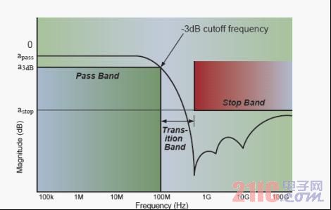
Figure 5: Single-Ended Low-Pass Filter Characteristics
Each component has a passband range, depending on the specification. These devices have a cut-off high frequency range from 700 MHz to 6 GHz.
The second type of EMI filter is suitable for high-speed serial interfaces and functions beyond typical low-pass filters. This type of interface is a differential signal path with inherent noise rejection, but does not fully immunize common mode noise from external sources or block interface signals from other parts of the system.
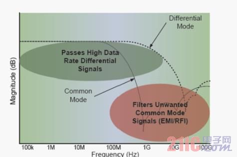
Figure 6: Common Mode Filter (CMF) Characteristics
A protected common mode filter (pCMF) can be used to eliminate unwanted common mode noise and to prevent radiated unwanted common mode noise signals from entering the rest of the system from the high speed interface. At the same time, it also allows high-speed data channels to be virtually undisturbed.
In addition to ESD strike protection, ON Semiconductor also offers solutions to protect against surges caused by lightning strikes or power-cross faults. The common interfaces in various consumer electronics and telecommunications/network equipment are RJ45 interfaces that comply with the 10/100BASE-T and 1000BASE-T Ethernet protocols, and their surge ratings are often indoor standards. These interfaces consist of four pairs of differential data lines, each capable of transmitting data rates up to 250 Mbps. The protection of this type of interface is required to ensure that lateral (metallic) surges do not damage sensitive downstream chips (such as physical layers). This is achieved by connecting the shunt protection elements to the line-to-line (each pair of wires) to transfer the incoming surge energy.
For lower data rate (10/100BASE-T) applications, ON Semiconductor offers a crowbar device combination called TSPD (Thyristor Surge Protection Device) and clamps for ESD-like protection. Device. TSPD offers the advantage of low clamping voltage and high inrush current capability. For example, these devices can meet the requirements of the GR-1089 10/1000 μs standard and are therefore suitable for primary or secondary protection, also known as "line-side" protection. TVS (Transient Suppression Diode) clamp devices support surge levels of 8/20 μs pulses, typically used on the tertiary or PHY side to capture and safely eliminate any residual surge pulses.
Typical Circuit Protection Application Example Smartphone applications are a typical protection application. ON Semiconductor's solutions include data filters, ESD protection diodes, and array and voltage protection devices. USB 2.0 protection for consumer and portable applications includes high-speed pairing, VCC and low-capacitance ESD protection; while USB 3.0 has two ultra-high-speed pairs and a high-speed pair, as well as VCC, low-capacitance ESD protection. The eSATA interface has two high speed pairs and low capacitance ESD protection.
Figure 7: Smartphone block diagram and I/O interface to be protected (see light blue background area on the lower right side)
For parallel interfaces to 4 to 12-line cameras and displays, ON Semiconductor has low-pass LC filters + ESD protection devices and 3 to 5 high-speed serial channel common-mode filters + ESD protection. For portable HDMI, consumer HDMI/display ports, four high-speed pairs, up to six additional interface lines, and low-capacitance ESD+ common-mode filter solutions are available.
In addition, ON Semiconductor's protection applications include audio (speakers/earphones), SD interfaces, SIM cards, keyboard EMI suppression, Ethernet, and T1/E1, T3/E3 and xDSL ports to meet consumer electronics Powerful ESD protection and higher requirements for reducing EMI/RFI noise.
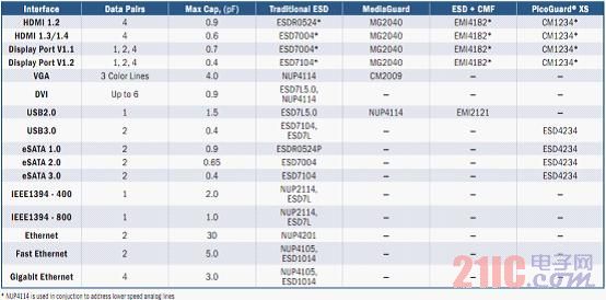
A strong line of ESD protection and EMI filtering products for portable and consumer application interfaces. ON Semiconductor is the premier silicon solution provider for energy-efficient electronic products in the world, ranking first in the circuit protection market for portable and wireless, consumer, computer and The market for peripherals, automotive and telecommunications offers a wide range of ESD protection and EMI/RFI filtering products. Tables 1 and 2 list the ESD protection and EMI filtering solutions used by ON Semiconductor for portable application interfaces and consumer application interfaces. Customers can select the appropriate solution based on actual application requirements.
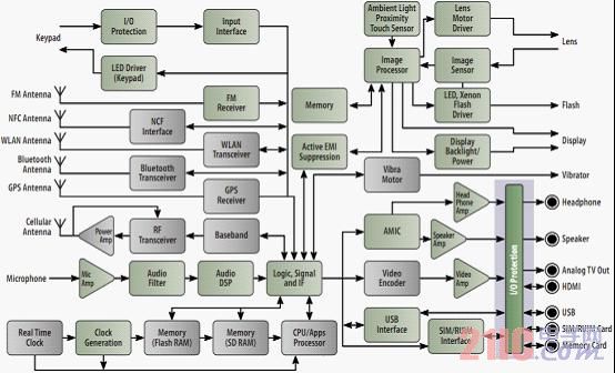
Table 1: ON Semiconductor's portable application interface ESD protection and EMI filtering solutions
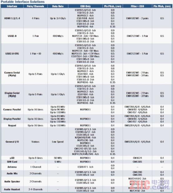
Table 2: ON Semiconductor's consumer application interface ESD protection and EMI filtering solutions
to sum up:
ON Semiconductor is a global leader in circuit protection. Leading ESD protection products include: the industry's lowest capacitance, very low clamping voltage for traditional ESD protection solutions; the first PicoGuard XS protection solution on the market that provides zero capacitance. And the same common ESD protection common mode filter solution introduced in the market. These highly integrated protection solutions help customers protect sensitive chipsets in their products and reduce board space.
Binding Post refers to the terminal installed on the power amplifier and Speaker box for connection with the speaker line.
Post type specification editor
Hexagon | | plum blossom nickel/silver plated JXZ - type 1 terminal/JXZ - 2 miniature terminal/JXZ - 2 (â…¡) terminal/JXZ - 2 (silver)/terminal/metal grounding column JXZ - 3 (a) 30 type terminal/JXZ - 3 (a) 50 type terminal/JXZ - 3 terminal/JXZ - type (100 a) 4 (a) 30 type terminal/JXZ - 4 type terminal/JXZ - 4 (100 a) terminal/JXZ - 4 (50 a groove terminal/ jxz-4 (100A aperture terminal/jxz-200a terminal/jxz-600a high-current terminal )

Binding Post
Binding Post,Electrical Conductivity Binding Post,Terminal Connector Binding Post,Double Electrical Binding Post
Ningbo Best Group Co.,Ltd , http://www.speakerbuzzer.com