This article brings you the design of the intelligent electronic scale system using AT89S52 single-chip microcomputer.
Introduction of AT89S52 MCUAT89S52 is an 8-bit single-chip microcomputer. The on-chip ROM adopts FLASH ROM technology. It is fully compatible with MCS-51 series. It can work with ultra-low voltage of 3V, and the crystal clock can reach up to 24MHz. The AT89S52 is a standard 40-pin dual in-line integrated circuit chip with four 8-bit parallel bidirectional I/O ports, denoted P0, P1, P2, and P3. The 31st pin needs to be connected to the high potential to make the MCU select the internal program memory; the 9th pin is the reset pin, which is connected to a power-on manual reset circuit; the 40th pin is the power supply terminal VCC, connected to the +5V power supply, the 20th pin For ground VSS, a 0.1μF high frequency filter capacitor is typically connected between the VCC and VSS pins. A 12MHz crystal oscillator is connected between pins 18 and 19 to provide a clock signal to the microcontroller.
AT89S52 type MCU pin function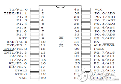
VCC: power supply voltage
P0 port: P0 port is a set of 8-bit open-drain type bidirectional I/O ports. When used as an output port, each pin can drive 8 TTL logic gate circuits. When writing 1 to port 0, it can be used as a high impedance input.
When the P0 port accesses the external program memory or data memory, it can also be set to the form of address data bus multiplexing. In this mode, the P0 port has an internal pull-up resistor.
During EPROM programming, the P0 port receives the instruction byte and the output instruction byte is at the time of program verification. An external pull-up resistor is required for program verification.
Port P1: Port P1 is an 8-bit bidirectional I/O port with internal pull-up resistors. The output buffer of port P can accept or output 4 TTL logic gates. When a 1 is written to the P1 port, they are pulled high by the internal pull-up resistor and can be used as an input. When used as an input, the P1 port has a pull-up resistor internally, so a low current (IIL) is output when the external is pulled low.
Port P2: P2 is an 8-bit bidirectional I/O port with internal pull-up resistors. The output buffer of port P2 can drive 4 TTL logic gates. When writing 1 to the P2 port, the port is pulled high by an internal pull-up resistor, which can be used as an input port. As an input port, because there is a pull-up resistor inside, a pin (IIL) is output when it is pulled low by an external signal.
When the P2 port accesses an external program memory or an external data memory of a 16-bit address (for example, MOVX @ DPTR), the P2 port sends high 8-bit address data. In this case, the P2 port uses a powerful internal pull-up resistor function when outputting 1. When an external data memory is accessed using an 8-bit address line (for example, MOVX @R1), the P2 port outputs the contents of the special function register. When the EPROM is programmed or verified, the P2 port simultaneously receives the upper 8-bit address and some control signals.
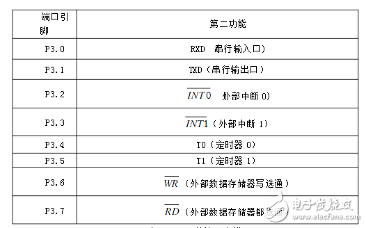
Port 3: P3 is an 8-bit bidirectional I/O port with internal pull-up resistors. The output buffer of port 3 can drive 4 TTL logic gates. When writing 1 to the P3 port, the port is pulled high by an internal pull-up resistor, which can be used as an input port. As an input port, because there is a pull-up resistor inside, a pin (IIL) is output when it is pulled low by an external signal.
The P3 port has a variety of special functions at the same time, as shown in the following table:
RST: Reset input. When the oscillator is operating, a high level of two machine cycles on the RST pin will reset the microcontroller.
ALE/PROG: When accessing external memory, the address latch allows an output pulse to latch the lower octet of the address. It can also be used as a program pulse output (PROG) when programming in Flash. In general, ALE is a 1/6 output of the crystal frequency and can be used as an external clock or timing purpose. Note, however, that an ALE pulse will be skipped each time an external data memory is accessed.
PSEN: Read strobe signal from the external program memory when the program is enabled. When the AT89C52 executes an external program memory instruction, each machine cycle PSEN is asserted twice, except that when accessing the external data memory, PSEN will skip both signals.
EA/VPP: External access allowed. In order for the microcontroller to efficiently transfer instructions from the 0000H to the FFFH unit of the external data memory, the EA must be connected to GND. The main thing to note is that if the encryption bit 1 is programmed, the EA terminal will automatically latch internally when reset. When executing an internal programming instruction, the EA should be connected to the VCC side.
XTAL1: The inverting amplifier of the oscillator and the input of the internal clock circuit. XTAL2: Output of the oscillator inverting amplifier.
LED Lighting Aluminum Alloy Die Casting
Led Lighting Aluminum Alloy Die Casting,Oem Aluminium Alloy Die,Led Zinc Die Casting,Aluminium Led Light Housing
Dongguan Metalwork Technology Co., LTD. , https://www.dgdiecastpro.com