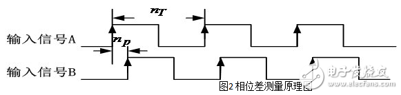
Figure 4: MCU Minimal System
The overall circuit diagram of the frequency and phase meter is shown in Figure 5: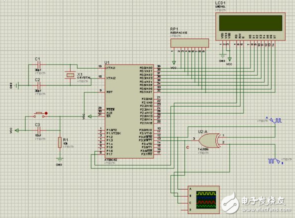
Figure 5: Overall Circuit Diagram of the Frequency Phase Meter
**Design Scheme Based on a Simple Digital Frequency Meter Using a Single-Chip Microcontroller (2)** This paper uses the prescaler SAB6456A and high-speed digital divider 74HC390, combined with the new MSP430F449 microcontroller, to propose a novel, fully automatic digital display RF frequency measurement design.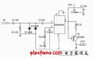
Figure 1: Signal Front-End Processing and Frequency Dividing Circuit
**Main Device Introduction** **MSP430F449 Microcontroller** The MSP430F449 features a 16-bit RISC architecture with extensive on-chip peripherals and high-capacity working registers and memory, offering a high price-to-performance ratio. Its key features include: - Ultra-low power consumption: Operates from 1.8V to 3.6V, with five low-power modes (LPM). In low-power mode, the CPU can be awakened by interrupts within less than 6μs. - Strong computing power: 16-bit RISC structure, rich addressing modes, 16 interrupt sources, and up to 125ns instruction cycle at 8MHz. Includes an internal hardware multiplier, 64KB Flash, and 2KB RAM. - Rich on-chip peripherals: Watchdog timer, basic timer, comparator, 16-bit timers (TA, TB), serial ports, LCD driver, 6×8-bit I/O ports, and 12-bit ADC (up to 200kHz sampling rate). - Convenient development environment: Flash-based device with JTAG interface for program download and debugging without an emulator or programmer. **Prescaler SAB6456A** The SAB6456A is a prescaler designed for UHF/VHF frequencies. It can divide input frequencies from 70MHz to 1GHz by 64 or 256, depending on the MC pin status. High sensitivity and strong harmonic suppression make it ideal for RF applications.
Figure 2: MCU Peripheral Circuit
**Working Principle** The design consists of two main parts: frequency division and counting. First, the input signal is clipped and divided by the SAB6456A. Then, the 256-divided signal is further divided by two 74HC390 high-speed dividers, converting the analog signal into a low-frequency digital signal below 10kHz. This signal is then fed into the MSP430F449 MCU, which uses its 16-bit timer A for timing and counting. The timer has several functions, including a counter section, capture/compare registers, and an output unit. Using the continuous counting mode and rising edge capture mode, the time of N pulse signals is measured in the timer interrupt, and the frequency is calculated by dividing N. **Hardware Design** Figure 1 shows the front-end processing and crossover design of the signal. The output signal is divided by two SN74HC390s, each capable of dividing up to 50MHz. Connecting them in series allows a total division of 1000, reducing the signal frequency to about 4kHz or lower, suitable for direct counting by the microcontroller. Figure 2 shows the peripheral circuit of the microcontroller, including the reset circuit, power supply, and crystal oscillator necessary for operation. The crystal oscillator provides 8MHz and 32.768kHz signals, with 8MHz used as the timer A input clock and 32.768kHz for the digital tube display. The 74LS373 is a D-type latch that can directly drive common cathode digital tubes due to its high output current. **Software Design** The divided output terminal OUT is connected to the frequency input of the MCU. After a delay to stabilize the signal, the program opens the capture interrupt and timer A, counts N pulses in the timer A interrupt, and calculates the frequency by dividing N. The result is multiplied by the frequency division coefficient to get the actual frequency, which is then displayed. After a short delay, the process repeats. When measuring low-frequency signals, the LED display is turned off to ensure accuracy. For such cases, fewer pulses are measured or the delay is reduced to minimize average measurement time. Dynamic scanning display works by sending scanning signals to each digit one by one via P4, while P3 inputs the segment data to drive the digits. This ensures that each digit is displayed sequentially, with a display time of more than 1ms, preventing visible flicker. **Main Measurement Procedure:** ```c void frequency_measure(void) { float tmp, tmp1; Key_flag = 0; // Clear button flag P1OUT |= BIT0; Delay(1000); // Wait for signal stabilization while (1) { IE2 &= ~0x80; // Disable BT, turn off LED Firstflag = 1; // Start measuring first pulse TACTL |= TAIE; // Enable capture CCTL1 |= CCIE; // Enable Timer A while (f_ok_flag == 0); // Wait for measurement end f_ok_flag = 0; if (aa1 != aa2) { overflow--; } tmp = aa2 - aa1; tmp1 = 40.0 / (overflow * 0.008191875 + (tmp / 8000000.0)); result = tmp1 * 0.256; IE2 |= 0x80; // Enable BT, turn on LED Yanshi(2, 2); // Adjust delay here CCTL1 &= ~CCIE; // Disable capture TACTL &= ~TAIE; // Disable Timer A return; } } ``` The flowchart is shown in Figure 3.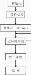
Figure 3: Main Program Flow
**Conclusion** The hardware and software described in this paper have been tested in practice, and the results show high measurement accuracy. The instrument is cost-effective and has a simple structure, making it an economical frequency tester. **Design Scheme Based on a Simple Digital Frequency Meter Using a Single-Chip Microcontroller (3)** The digital frequency meter measures frequency using timing and counting, and dynamically displays 6 digits on a 1602A LCD. The measurement range includes sine, square, and triangle waves from 1 Hz to 10 kHz, with a time base width of 1 μs, 10 μs, 100 μs, and 1 ms. The microcontroller enables automatic measurement functionality. **Design Idea and Frequency Calculation of the Frequency Measuring Instrument** The design involves dividing the signal, measuring the number of cycles of a known standard frequency signal over one or several measured signal periods, and then calculating the frequency. The principle is illustrated in Figure 1 on the right.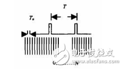
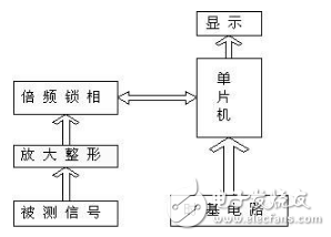
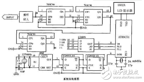
Figure 3: Digital Frequency Meter System Working Principle Diagram
**Signal Conditioning and Amplification Shaping Module** The amplification shaping system includes an attenuator, follower, amplifier, and Schmitt trigger. It converts a sinusoidal input signal Vx into a square wave Vo of the same frequency. The measured signal is divided and amplified to avoid waveform distortion. An operational amplifier-based emitter follower increases the input impedance. The non-inverting op amp has a gain of (R1 + R2)/R1, adjustable by changing R1. The shaping circuit uses a Schmitt trigger, and the shaped square wave is sent to the gate for counting. Since the input signal amplitude is uncertain, it may be too large or too small, causing damage or failure to detect. Therefore, the signal conditioning circuit performs impedance transformation, amplification, limiting, and shaping. The circuit schematic and parameters are shown in Figure 4: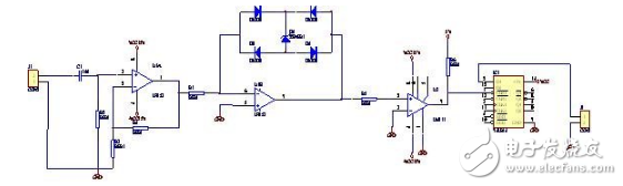
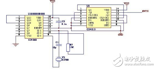
Figure 7: Second Pulse Generation Circuit Schematic
Radiators in this case are manufactured with Stainless steel (SS304, SS316 and SS316L).
These radiators are manufactured with both 1mm CRCA sheet and 1.2 mm CRCA sheet as required and centre distance varying from 600 mm to 4000 mm. Stainless steel radiators can be offered with and without paint.
Through the method, the stainless steel plate type radiator for the transformer is simple in structure, free of complex treatment process on the surface of the radiator, not prone to oxidizing and corroding, long in service life, and high in welding strength.
Stainless Steel Radiator,Stainless Steel Transformer Radiator,Stainless Steel Cooling Radiator,Stainless Steel Weather Proof Radiator
Shenyang Tiantong Electricity Co., Ltd. , https://www.ttradiator.com