Introduction
Wireless communication networks are rapidly developing. Consumer demand for enhanced data services is growing, and bandwidth usage is rising. Next-generation wireless communication systems require higher data throughput rates, lower power consumption, and higher reliability. These requirements usually conflict with each other. To meet these requirements, a digital-to-analog converter (DAC) solution with high sampling rate, high signal bandwidth, and high efficiency is required. The new generation of high-speed DAC products with GSPS sampling rate and input data rate provide multi-carrier GSM-compatible performance for multi-band, multi-standard radio base stations while reducing overall system power consumption and thermal density. This article discusses how high-speed converters can help system designers drive innovation in wireless communication systems with higher sampling rates, wider data bandwidth, and lower power consumption.
High-bandwidth challenges to the system It is not uncommon for modern mobile base stations to have transmission bandwidths in excess of 300 MHz. To support the requirements of wider data bandwidth and digital pre-distortion technology, the standard signal bandwidth and dynamic performance standard requirements for high-speed DAC products have been increased. In order to achieve higher system bandwidth, there are three challenges.
First, higher signal bandwidths require faster DAC sampling rates. Nyquist-Shannon sampling theory states that the converter sampling rate should be at least twice the frequency of the signal to be synthesized. Therefore, without considering other design constraints, the DAC sampling rate needs to be increased at a rate twice the signal bandwidth. Moreover, analog reconstruction filtering is another important factor in system design. In order to simplify the design of this filter, a higher DAC sampling rate is required. The use of a rectangular analog filter in a wireless transmitter is neither feasible nor effective. In practice, the system requires a certain oversampling ratio of the DAC sampling rate relative to the composite signal bandwidth to construct a filter transition between the target signal and the high frequency DAC sample image that needs to be suppressed. For example, if the signal bandwidth to be synthesized is ±50 MHz and the center frequency is 150 MHz, the upper limit of the DAC output signal is 200 MHz; and if the signal bandwidth to be synthesized is ±150 MHz and the center frequency is 300 MHz, the DAC output The upper limit of the signal is 450 MHz. It can be seen that the second case requires much higher DAC sampling rate.
Second, higher signal bandwidths require converter data interfaces to be faster and more reliable. The required signal bandwidth is increased in proportion to the throughput rate of the transmitted data. To achieve 300 MHz system bandwidth with IQ modulation, the combined input data rate for a dual DAC (I and Q) needs to be 750 MSPS (assuming a filter roll-off factor of 0.2). Therefore, the input data period is 1.33 ns, and the timing misalignment of the data bus must be eliminated as much as possible to meet the setup and hold timing requirements, which puts tremendous pressure on the system designer. If traditional parallel data interface schemes, such as LVDS and CMOS, are used, the implementation will be very difficult. The new JESD204B high-speed serial interface provides a reliable and scalable solution that supports upgrades to higher data rates.
Third, integrated circuit (IC) devices are not ideal devices. DAC is no exception. Higher output bandwidths require better dynamic performance for DAC devices for two reasons: First, the dynamic range generally decreases as the DAC output frequency increases. In addition, when the bandwidth is large, there are often more spurious components falling into the target frequency band. However, system spur requirements do not increase or decrease as the signal bandwidth increases. No matter how much signal bandwidth is supported, the mobile base station must meet the emission template requirements. A DAC with excellent dynamic performance simplifies the frequency planning and filtering of the system.
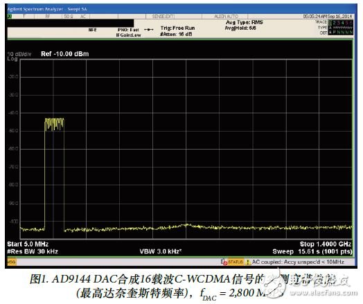
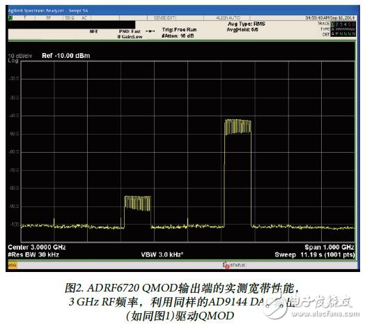
Figure 1 and Figure 2 show the measured spectral performance of the AD9144 DAC combining an 80 MHz signal (16-carrier C-WCDMA) at a DAC sampling rate of 2,800 MSPS.
System Low Power and High Reliability Challenges To increase transmit bandwidth and data capacity, system designers face other challenges, including power, cooling, and system reliability. These aspects are often not conducive to achieving higher system bandwidth, and sometimes even conflict with this goal. As a result, system designers need a new DAC that can achieve higher feature integration, lower power consumption, lower operating heat density, and wider bandwidth in the same package.
High-speed DAC products have grown rapidly in recent years and have integrated more digital and analog features. The DAC on-chip clock multiplier PLL and communication-specific signal processing features are two prominent examples. In the past, these features were implemented elsewhere in the system, such as high-speed clock synthesis chipsets and baseband ASICs/FPGAs. A DAC with these features not only reduces total BOM cost, but also simplifies design and increases reliability. Due to the built-in clock multiplier of the DAC, the system only needs to provide a low frequency reference clock for the device. The clock multiplier locks the external reference clock and produces a high-speed sample clock for use inside the DAC. This reduces concerns about high-speed clock coupling and PCB trace impedance matching. New digital features such as power detection and protection provide additional protection for the RF signal chain from over-range signals or abnormal system behavior. Despite the significant increase in integration, the power consumption of DAC devices has remained roughly stable or even reduced compared to previous generations, thanks to the smaller silicon node size and the advancement of high-speed DAC technology, which has played a role in solving these system challenges. Great role.
In addition to lower power consumption and lower carbon emissions, another major benefit of low power devices is lower heat density. Wireless communication systems are typically confined to watertight, sealed metal enclosures. Size and weight restrictions generally do not allow for active cooling. The heat generated by the IC device needs to be dissipated through the chassis. The cavity and PCB temperatures inside the chassis can be so high that they can affect the long-term reliability of the system. The accumulated heat may affect the mechanical properties of the PCB, the solder joint between the device and the board, and accelerate the aging, that is, the electrical characteristics of the IC device may also cause long-term shift. The heat distribution/heat dissipation in the system is not uniform, and the heat generation is mainly signal-intensive devices, and the high-speed DAC is one of them. Therefore, feature-rich, low-power DACs are attractive to system designers.
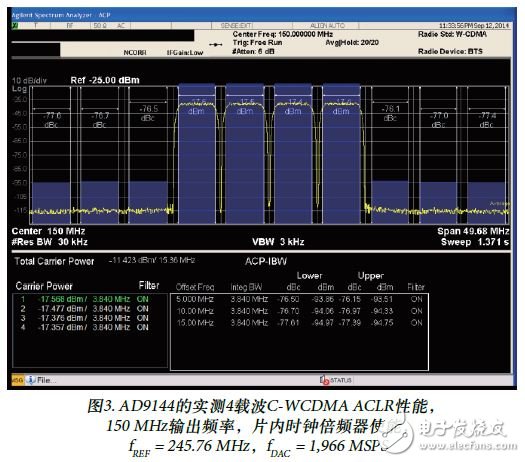
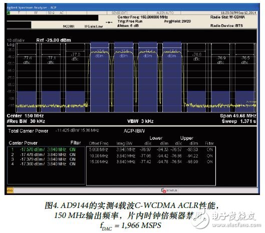
Figure 3 and Figure 4 show the measured performance of a 4-carrier C-WCDMA signal synthesized with the 1966 MSPS DAC sampling rate with the AD9144 turning on and off the DAC on-chip clock multiplier, respectively.
The challenge of the system in the design of a common platform While requiring wider coverage and wider bandwidth, the rapid expansion of consumer demand for data services requires the support of multi-standard radio (MSR) base stations. Different radio technologies and increasing frequency allocation make control networks and cost reductions more complicated. In order to meet these needs, the MSR base station construction problem must be solved through an efficient and relatively inexpensive solution, namely a common platform design. Advances in DAC technology support this development in base station design. Multi-Carrier GSM (MC-GSM) is generally considered to be the most demanding air standard for dynamic range. MC-GSM testing is often used to determine whether a DAC product supports a common platform design.
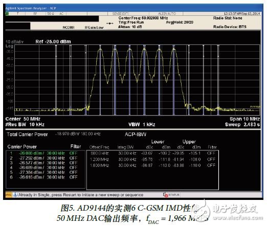
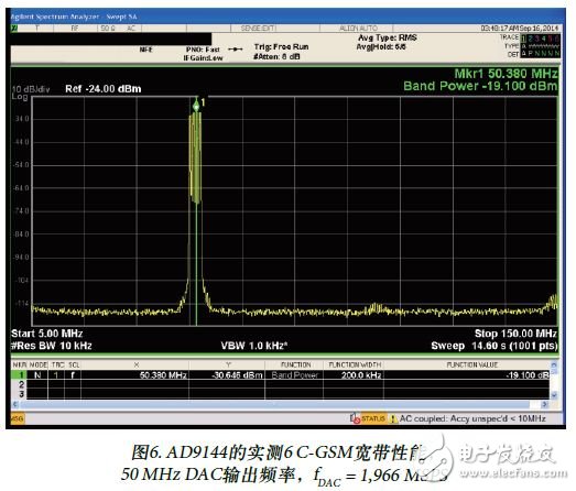
Figure 5 and Figure 6 show the measured performance of the AD9144 synthesizing a 6C-GSM signal at a DAC sampling rate of 1,966 MSPS.
Summary Modern wireless communication networks are moving toward more data services and higher bandwidth usage. To support this trend, next-generation wireless communication systems must have higher data throughput rates, lower power consumption, and higher reliability. Advances in high-speed DAC technology, such as the AD9144 from Analog Devices, can support next-generation multi-standard radio designs and have helped system designers achieve breakthrough innovation in multiple key technology dimensions.
About the Author
Yi Zhang is an applications engineer in the High Speed ​​Converter Division of Analog Devices. He joined Analog Devices in 2007 and has more than 8 years of experience in high speed converter products and high speed mixed signal applications. He has written data sheets, application notes, and technical articles for several generations of high-speed digital-to-analog converters (DACs). He holds a master's degree in electrical engineering from Cornell University.
Michele Viani is an applications engineer in the high-speed converter division of Analog Devices, Inc., and has been working for 5 years. He is both a product engineer and an application engineer responsible for evaluating high-speed digital-to-analog converter products and providing technical support to customers to solve implementation problems. He holds a bachelor's degree in electrical engineering from Rensselaer Polytechnic Institute.
Pin Header Connector,Pin Header Female,Male Header Pins,Right Angle Pin Header
Cixi Xinke Electronic Technology Co., Ltd. , https://www.cxxinke.com