After reading the first two articles, some students gave me a very good question on the WeChat public account: "Why is the wafer not square?" Yes, the square Die inside the round wafer is always inevitable and some space is wasted:
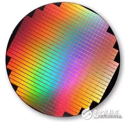
It’s a pity that the black area is wasted. If it’s not the party, is it all right? My answer to this question is: "Because the wafer is not called a crystal!"
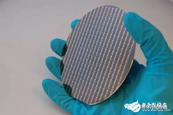
Hey, make a joke, but seriously speaking, the wafer is not completely round. The wafer you see is like this:
Why do I know the wafer is like this?
Or like this:
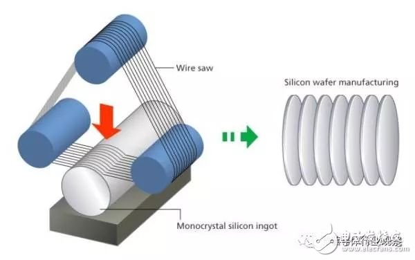
Because the production process determines that it is round. Because the purified high-purity polycrystalline silicon is grown by rotation on a seed. The polycrystalline silicon is melted and placed in a Quartz Crucible. After the subcrystals are placed in a crucible and rotated at a constant speed, the molten silicon will grow into a cylindrical ingot along the subcrystal. . This method is the CZ method (Czochralski), which is also used now, also called single crystal Czochralski. As shown below:

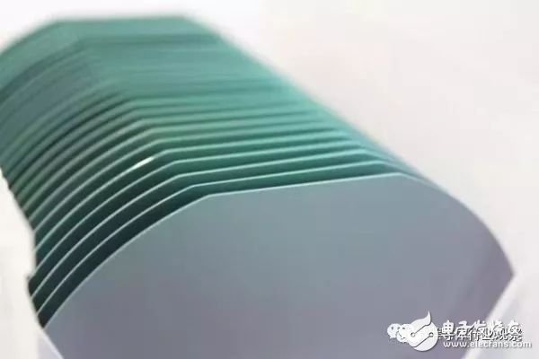
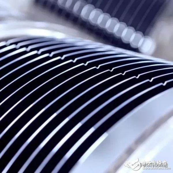
The silicon ingot is then cut into silicon wafers through a diamond wire:
After the grinding and so on, you can carry out the subsequent process (one of those things that the CPU manufactures: i7 and i5 are actually twin brothers!?)
The spin-up in the single crystal Czochralski process determines the cylindrical shape of the ingot and determines that the wafer is circular.
Why is it not rounded up later?That is why it is not round again? In fact, there is a process in the middle of it, that is Flat/Notch Grinning.
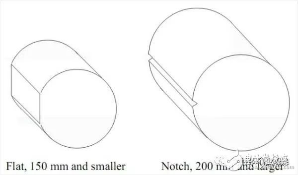
It will be carried out after the ingot is made. On a silicon ingot below 200mm, a flat angle is cut, called Flat. On a silicon ingot of 200mm or more, in order to reduce waste, only a small circular opening is cut, called Notch (Reference 2). After slicing, the wafer becomes like this:
If you look at my first picture carefully, you will also find that it is actually missing a small gap.
Why do you want to do this? Is this not a waste? In fact, this small gap is too close to the edge and is very small. It is destined to be useless when making Die. This can help the subsequent process to determine the Wafer placement position. For positioning, the crystal orientation of the single crystal growth is also indicated. The pointing device can look like this:
This kind of cutting, testing is more convenient.
in conclusionIn the strict sense, all Wafers are not round. If you ignore the small problems of Flat/Notch, then its circle is determined by the process.
Pvc Control Cable,Screen Control Cable,Steel Tape Armor Control Cable,Armor Control Cable
Baosheng Science&Technology Innovation Co.,Ltd , https://www.bscables.com