Abstract : This paper introduces the application of military electronic system application using the domestic Godson 3A multi-core processor and related bridge chip, with VXWORKS operating system and image processing software, in order to explore the application of domestic multi-core processor in military electronic system; The system has various functions such as image processing, serial port, SATA, network port, USB and other interfaces and PMC interface expansion. It can input video images through USB interface, use software algorithm for real-time processing of multi-core images, and VGA interface for video output display. It provides design for meeting the requirements of integration, integration, miniaturization, low power consumption and localization of military electronic systems. reference.
This article refers to the address: http://
0 Preface
Multi-core processor, with multi-core redundancy and parallel processing of each thread without hang, small size, high integration, etc., can adapt to the development of military embedded systems integration, miniaturization and low power consumption, so in military applications It has special value; P2020 multi-core processor has been successfully applied in an aviation integrated data processing module.
This application adopts domestic Loongson 3A multi-core processor, which performs PMC sub-card data processing and video image parallel processing through sub-verification processing, and realizes communication of peripheral interfaces such as network port, serial port, USB, SATA and VGA through bridge expansion. Transmission function; can pass the USB2.0 interface to the incoming video image and the PMC data input into the PMC socket in parallel, and process the result in real time through the VGA interface and the PMC socket. With the continuous development of chip technology and application level, domestic multi-core processors will provide a strong guarantee for the localization of military systems.
1 system design requirements
The system needs to receive video images through the USB2.0 interface, and is output from the VGA port after being processed by the multi-core processor. The interface expansion and data processing functions can be realized through the standard PMC interface. It also has USB, serial port, network port and SATA interface communication extension transmission function.
2 system architecture
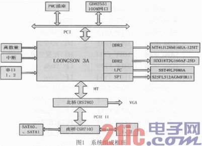
This design adopts the multi-core feature of the Godson 3A processor, and distributes the core 1 and the core 2 to perform the functions of PCI bus expansion and video image processing respectively; the network port function is extended by the network port chip GD82551. This project expands AMD's North Bridge chip RS780E through HT interface to realize VGA display interface expansion. It realizes the expansion of USB2.0 and SATA interface through PCIE for South Bridge SB710 chip expansion.
The RS780E is a Northbridge chip introduced by AMD. It supports multi-core functions, on-chip integrated graphics and image functions, multiple display interfaces, supports different refresh rates, and supports high-speed HT3 interface and PCIE expansion. The SB710 is a South Bridge chip for the RS780E and supports USB, SATA and PCIE functions.
The video image is input to the SATA extended storage disk via the USB interface, and then processed by the Longxin 3A multi-core processor for character superposition, brightness, contrast adjustment, etc., output from the VGA interface on the north bridge, and discrete through the GPIO interface of the Loongson 3A. The input and output of the quantity and interrupt signal are debugged and displayed through two serial ports. The block diagram of its system is shown in Figure 1.
3 detailed design
3.1 Introduction of Godson 3A Processor
The Godson 3A processor is the first product in the Loongson multicore series. It is manufactured in a 65nm process and integrates four 64-bit superscalar general-purpose processor cores in a single chip. The maximum operating frequency is 1GHz, and the maximum power consumption is 15W. The energy efficiency ratio is 1.06Gflop/W. It is twice as large as the X86 series processor. The main features are as follows:
(1) Four 64-bit four-transmit superscalar GS464 processor cores are integrated on-chip; it is a general-purpose RISC processor that can implement the 64-bit MIPS64 instruction set. The instruction pipeline takes four instructions per clock cycle for decoding and dynamically transmits it to five full-flow functional components;
(2) On-chip integrated quad-core shared 4MB secondary cache;
(3) Integrate two 64-bit 400MHz DDR2/3 controllers;
(4) Integrate two 16-bit 800MHz HyperTransport controllers;
(5) On-chip integrated 32-bit 33MHz PCI/PCIX;
(6) One LPC, two UARTs, one SPI, and 16 GPIO interfaces are integrated on-chip;
(7) Support multi-core chips through the HyperTransport interface interconnection and cross-chip global Cache consistency;
(8) The running frequency is up to 1GHz, the design is realized as 800MHz, and it can be configured.
3.2 Multi-core selection
The overall architecture of the Godson 3A processor chip is interconnected based on the two-stage crossbar switch as shown in Figure 2.
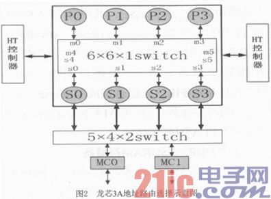
The first-level interconnect switch uses a 6×6 crossbar switch for connecting four CPUs (as a master device); each IO port is connected to a 16-bit HT controller, and each 16-bit HT port can also be used as two An 8-bit HT port is used. The HT controller is connected to the primary interconnect switch through a DMA controller, which is responsible for IO control of the IO and is responsible for the maintenance of inter-chip consistency.
The second-level crossbar switch uses a 5×4 crossbar switch to connect four secondary Cache modules (as master devices), four secondary Cache modules (as slave devices), and two IO ports (one master and one for each port). A Slave), crossbar switch connects two DDR2 memory controllers, low-speed high-speed I/O (including PCI, LPC, SPI, etc.) and the internal control register module.
By setting the two-stage crossbar switch register, the core 1 and the core 2 respectively perform the PMC daughter card data processing and the parallel processing of the video image. The data channel with read and write separation, the data channel width is 128bit, and works at the same frequency as the processor core to provide high-speed on-chip data transmission.
3.3 Storage Circuit Section
Two pieces of FLASH memory SST49LF080B with LPC interface are respectively connected to the LPC interface of the processor of Godson 3A for storing the PMON program of Loongson; two serial ST SPI FLASH memories S25FL128SAGMFIR11 are used to store the operating system and test program, and use The HT1 interface is connected to the north bridge chip for VGA interface expansion, and then the HT interface of the north bridge is connected to the HT interface of the south bridge for USB and SATA port expansion, and the external SATA FLASH is used to store video and other related data; using two DDR3 SDRAM memories MT41J128M16HA-125IT, the capacity is realized. Each is 2G and is used to build internal memory.
3.3.1 FLASH memory circuit
The module uses three pieces of FLASH, of which SST49LF080A is a FLASH chip with LPC interface and capacity of 8Mbit (1024k×8 (8Mbit)). It can be used to store PMOON program and can be erased by parallel port. The other two pieces have FLASH with SPI interface. The chip S25FL512SAGMFIR11 is a combined 64Mbyte storage space for storing operating system programs: FLASH extended storage is implemented by using the SATA NANDrive FLASH electronic disk.
3.3.2 DDR2/3 SDRAM Memory
The Godson 3A multi-core processor has two DDR2/3 SDRAM memory controllers, provides DDR3 timing control logic, and provides DDR3 access clocks. Both CPU and PCI masters can access DDR3 SDRAM.
The solution is implemented with 256MB capacity DDR3 memory particles MT41J128M16HA-125IT, the working voltage is 1.5V, and the maximum operating frequency is 667MHz.
In order to support different DDR3 SDRAM granules in the system, DDR3 SDRAM needs to be configured after power-on reset. The memory initialization sequence is as follows: during system reset, all register contents will be cleared to the default value; then the system reset is released, and then the configuration register address is Send 64-bit write instructions to configure all 29 configuration registers. If you write CTRL 03 at this time, you should set the parameter START to 0. All registers must be properly configured for proper operation. Then send a 64-bit write command to the configuration register CTRL 03. The parameter START should be set to 1 at this time. After the end, the memory controller will automatically initiate an initialization command to the memory.
3.3.3 Memory Address Allocation
The system physical address distribution of the Godson 3A processor uses a globally accessible hierarchical addressing design to ensure extended compatibility of system development. The physical address width of the entire system is 48 bits. According to the upper 4 bits of the address, the entire address space is evenly distributed to 16 nodes. The Godson 3A uses a single-node 4-core configuration.
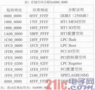
Within each node, the 44-bit address space is further evenly distributed to possibly up to eight devices connected within the node. The lower 43-bit address is owned by four Level 2 Cache modules, and the upper 43-bit address is further distributed to the devices connected to the four-direction port by the [43:42] bits of the address. Different from the mapping relationship of the directional ports, the cross-addressing mode of the secondary Cache can be determined according to the access behavior of the actual application. The four level 2 Cache modules in the node correspond to a 43-bit address space, and the address space corresponding to each level 2 module is determined according to a certain two-bit selection bit of the address bits, and can be dynamically configured and modified by software, and its memory space The assigned address is shown in Table 1.
3.4 Interface design
The system provides a 10MB/100MB fast Ethernet interface, which is controlled by the Godson 3A chip to control the GD82551 network port chip expansion; the serial communication interface is provided by the UART serial debugging interface integrated in the processor, and the maximum rate can be set through the chip. The processor contains 16 GPIO general-purpose I/Os as discrete interfaces. The module's 1 external discrete input signal, 3.3V level GSE#, is defined by software.
In addition, Godson 3A provides a JTAG-compatible boundary scan EJTAG interface for testing whether the processor pins are properly connected for debugging the underlying application software; airborne PMC daughter card and video image processing via the SATA interface on the south bridge The module's electronic storage disk expands; the PMC data is input and output through a dedicated PMC socket, and the USB interface can perform video image input and USB device connection, and the VGA interface performs processing of the video information after processing.
3.5 power circuit
The power required for the Godson 3A processor is six types: 1.1V, 3.3V, 1.8V, 0.9V, 2.5V, and 1.7V. Using five LTM4616 chips to configure the high-precision resistor output, the output configuration formula of the LTM4616 chip is as follows:

The processor core voltage is 1.1 V, and the maximum current is 12.8 A. It is realized by 5V parallel connection of LTM4616 two outputs, and the maximum 16 A can meet the requirements of use. 3.3V, 1.8V is a group, 0.9V, 2.5V is a group, 1.7 V is a separate group and can be generated by a single piece of LTM4616.
The 1.8V VDD and VDDO power supplies required for DDR2 are provided by MT47H128M16HG-3; the 0.9V VREF and VTT are provided by the power conversion chip TPS51100 with 3Asink-souce function. The SB710 and RS780 need to provide +1.2V power supply and one LTM4616.
3.6 clock circuit
The clock signals required by this module include: processor clock, north-south bridge clock, memory clock, and interface circuit (SATA, USB) clock.
The five system input clock signals of the processor are: SYSCLK, MEMCLK, PCI_CLK, HTCLK, differential clock HT0_CLKp/HT0_CLKn, and HT0_CLKp/HT1_CLKn.
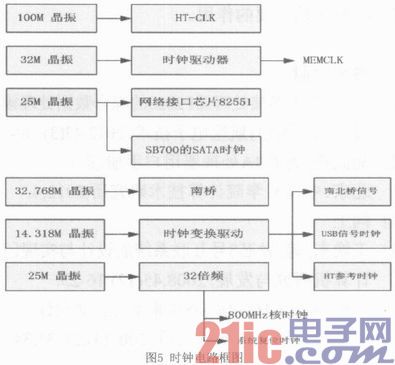
The core Core clock of Godson 3A is generated by SYSCLK, and the DDR2/3 clock is generated by MEMCLK. HT's single-ended clock HTCLK100MHz is generated using a crystal oscillator SG-8002CA-100MHz-PCB.
The south and north bridge clocks are generated by the S3188 625TTR chip using the 14.318MHz crystal oscillator: the CK_14M_NB and CK_14M_SB clock signals are sent to the North Bridge and the South Bridge respectively. The south bridge's USB clock, HT reference clock, and 32.768MHz crystal oscillator provide clocks to the SB700 to generate SATA clock signals, as shown in Figure 5.
3.7 Reset circuit
The reset circuit includes a processor reset, a south and north bridge reset, and a power-on reset.
The global reset signal of the circuit module processor is SYSRESETn: this reset signal is the only global reset signal. SYSCLK and CLK must remain stable until SYSRESETn is released to inactive. The valid time of SYSRESETn must be greater than one clock cycle. It is implemented by programmable logic. The internal reset control logic of the processor starts to reset the processor when SYSRESETn is invalid.
The system reset circuit is implemented by MAX708TESA. The MAX708TESA provides a sense of the supply voltage and the MAX708TESA can simultaneously generate a low level.
* and high level two reset signals (RESET), MAX708TESA monitors +3.3V voltage, when +3.3V voltage is lower than 3.08V, the reset output is valid. Also available is a PFI input designed to monitor the 5V level of the external supply, when the 5V input is below 4.65V,
The output is valid and this signal can be used as an external interrupt source for the Godson 3A processor.
The north bridge reset signal SYSRESET group is from the reset chip; POWERGOOD is the power OK input signal, input from the FPGA; LDTSTOP# is from the south bridge HT state transition enable signal; ALLOW LDTSTOP is enabled by the south bridge input north bridge to allow the LDT STP# to insert the signal. The logic relationship between the reset signals is generated by the programmable logic chip XC95288XL-7TQG144I.
3.8 Interrupt circuit
The pin interrupt of the Godson 3A processor includes 4 system interrupts (INTn), 4 PCI interrupts (PCI_IRQ), 2 PCI bus error reporting signals (PCI_SERRn and PCI_PERRn) and 1 non-maskable interrupt (NMIn).
This design uses the Loongson internal interrupt controller to handle interrupts such as serial port and PCI bus. PMOON is responsible for completing the interrupt number application and routing of PCI/PCIE devices and slots on the bridge. The operating system completes the allocation of interrupt numbers and interrupts within the chip. Routing and setting up the interrupt controller inside the chip.
The four system interrupt (INTn) pin interrupts of the Godson 3A processor are input to the network interface interrupt, serial port interrupt and two external interrupts respectively. The non-masked interrupt is connected to the MAX708 power supply monitor. When the external 5V falls below 4.65V, the non-masked interrupt is generated. . All external interrupt sources are level triggered and active low.
3.9 Other considerations
The processing board is a high-speed signal processing board. Space:Height is taken during the PCB design process for signals without special instructions.
1:1; GND via vias, decoupling capacitors as close as possible to the chip's power and ground pins, large areas of copper and other means to ensure signal quality.
In addition, the environment adaptability of the chip, such as the Godson 3A processor, fails to meet the requirements of the military's rigor. Therefore, it is necessary to use the vibration damping and temperature control components in accordance with the specific conditions.
USB video sources are widely used in mobile applications such as mobile phones, so that high-definition USB video sources have emerged. Domestic USB2.0 video image processing chips are developing rapidly. Civil USB video sources are very mature, with the introduction of USB3.0. The relevant domestic units are also stepping up exploration and development of military video source applications. At present, civilian USB video source plus ring control can be temporarily used to provide military USB video source, and video transmission can be performed through the network.
4 software system
The software system of the processor module includes: boot software, BIT test program, operating system and application software program.
The initialization boot program uses the PMON program that combines the BIOS and the boot program that comes with Loongson. It is initialized in two stages: the first stage runs in ROM FLASH, mainly for basic hardware initialization, such as: North Bridge, South Bridge, Memory Control Second, in the memory, the second phase is executed in memory, mainly to complete the environment variables, basic data structure, PCI bus, device initialization, network protocol and device initialization, and to drive the device on the searched PCI bus. Loading and configuration, etc., finally loading the operating system kernel.
The Loongson multi-core processor core 1 functions as the main processor and the core 2 to perform the parallel processing of the PMC sub-card data processing and the video image respectively. The startup process of the main processor is basically the same as the startup process of the single-core system. Mainly complete the startup of the processor core, TLB, MMU and related peripherals. The slave processor executes according to the polling loop.
The operating system uses the VxWorks 6.7 operating system to develop application software applications under linuxVxWorks 6.7.
The BIT adopts the power-on BIT, which mainly completes the system check when the product is powered on, and detects the core resources required for the system operation.
After the system is started, all processor cores will enter the reset exception program in BOOT.S in PMON to determine whether the master or slave processor enters different program branches. If it is the main processor, it initializes the CPIO configuration register, the clock frequency, the local io register, and then performs the main processor initialization work, including setting the interrupt, initializing the DDR register, LPC, etc., and then entering the execution of the operating system program. The work of the core in PMON is basically completed. Then, the slave processor initializes the slave processor's core, sets the processor cache coherency protocol and the cache of the KSEGO segment access, and then initializes the MMU and TLB related registers, and then obtains the current slave processor ID number, and obtains the IP_STATUS address, and then Check if the value in the corresponding mailbox is not 0. If yes, set the stack pointer and enter the operating system.
The application software performs processing such as contrast and brightness conversion on the video image output by the USB camera, and outputs it through the VGA port after processing.
The data format of the USB video image is not the familiar RGB24 format, but contains 12 bytes of frame headers per frame header (FF, FF, 00, C4, C4, 96, 00, XX, XX, XX). , XX, XX), and the data format of each frame is the so-called Bayer mode (which is applied to CCD and CMOS cameras). It allows color images to be obtained from a single plane, which can be converted to RGB24 format by writing a corresponding conversion program to decode the video data through software decoding.
5 Summary
This project studies the application of the dual-function of the PMC daughter card expansion function and the video image processor in the parallel embedded real-time implementation of the Loongson-made 3A multi-core processor in the military embedded system. With the continuous development of the chip technology and application level, the domestic multi-core processor It will play an increasingly important role in meeting the generalization, integration, integration, miniaturization and low power consumption of military systems.
Pluggable Terminal Block is made of two parts of pluggable connection. One part compresses the wire and then plugs it into the other part, which is welded to PCB. The mechanical principle of the connection bottom and the anti vibration design ensure the long-term airtight connection of the product and the use reliability of the finished product. The two ends of the socket can be equipped with matching ears, which can protect the connector to a large extent and prevent the poor arrangement of the connector. At the same time, this socket design can ensure that the socket can be inserted into the mother body correctly. The socket can also have assembly and locking positions. The assembly buckle can play a more stable role in fixing to the PCB, and the lock buckle can lock the mother body and the socket after the installation. Various socket designs can be matched with different insertion methods of the parent, such as: horizontal, vertical or inclined to printed circuit board, etc., and different ways can be selected according to the requirements of customers. Either metric wire gauge or standard wire gauge can be selected, which is the most popular terminal type in the market at present.
Our Pluggable Terminal block suit for 0.08mm² to 10mm² wire connection with 2.5mm to 10.16mm pitch. Flexible wire insert direction. connect direction and plug-in direction according to customer requirement.
Pluggable Terminal,Pluggable Terminal Block,Pluggable Terminal Block Connector,Pcb Pluggable Terminal Block Connector
Suzhou WeBest Electronics Technology Co.Ltd , https://www.webestet.com