1 Introduction
The step-down integrated switching power supply controller is widely used in various portable devices. In recent years, with the improvement of performance and functions of battery-powered portable devices, such as mobile phones, MP3 players, PDAs, higher and higher requirements have been placed on the efficiency of switching power supplies.
To increase efficiency and reduce off-chip components, current Buck converters typically integrate power switches and synchronous rectifier switches. At the same time, in order to reduce the size of the off-chip inductive components to suit the application of portable devices, the switching frequency is often set to the order of several megabits or more. The problem with this is that when the converter is operated under light load conditions, the switching losses become the main power loss. While portable devices work just in standby mode, that is, under light load conditions, light load efficiency is critical to extending battery life. Therefore, the issue of improving light load efficiency has received a lot of attention.
A common way to solve the above problem is to reduce the switching frequency under light load conditions so that the efficiency of the converter remains at a level similar to the heavy load. This technique has PFM/PWM multimode modulation, common gate drive, etc., but they have one common drawback: the switching frequency is modulated with the load, which makes the design of the off-chip filter quite complicated.
The green mode step-down power integrated switching power supply controller chip proposed in this paper adopts Burst/PWM multi-mode modulation technology. The control converter operates in PWM mode at a constant frequency under heavy load, and when the load is reduced to a certain level, it automatically Switch to Burst mode and work at a reduced constant frequency. Its main advantage is to reduce switching losses without increasing the design complexity of the off-chip filter. In addition, Burst mode can be enabled or disabled by user control depending on the needs of the application. And in the mode conversion process, the double reference method is used to achieve smooth transition and load hysteresis of mode conversion. At the same time, the chip introduces on-chip current sensing technology to replace the traditional resistance current detection, which reduces power consumption to some extent. The integration of power switches and synchronous rectification switches also simplifies the design of off-chip application circuits.
2 system design
The green mode step-down switching power supply controller proposed in this paper is a Buck converter with constant frequency operation and peak current control mode. The output voltage is adjusted by the off-chip voltage divider resistor. The power switch and synchronous rectifier switch are integrated on-chip. The system principle is shown in Figure 1.
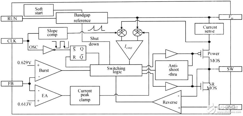
Figure 1 System schematic
2. 1 peak current PWM control mode
The control strategy of DC2DC converter mainly includes voltage type control and current type control. Compared with voltage type control, current mode control strategy is widely used due to its advantages of better linearity adjustment and simpler compensation circuit.
The authors propose a green-mode Buck converter that uses a peak current PWM control strategy when operating under heavy-duty conditions. Generally, according to different methods of inductor current detection, current mode control can be divided into different modes such as average current control, peak current control, and analog current control. The peak current control mode has fast transient response to changes in input voltage and output load. It has the advantages of instantaneous peak current limiting function and is the most widely used.
The peak current control loop is mainly composed of a current loop and a voltage loop. The working process of the control loop is shown in Figure 2. In the picture:
V sense = Vin - KIsense (1)
Where V in is the input supply voltage; V sense is the voltage signal detected by the current detection module; Isense is the signal detected by the detection module proportional to the inductor current. In addition, the V peak signal in Figure 2 is the voltage signal corresponding to the expected peak of the inductor current that is expected to be controlled by the voltage loop.
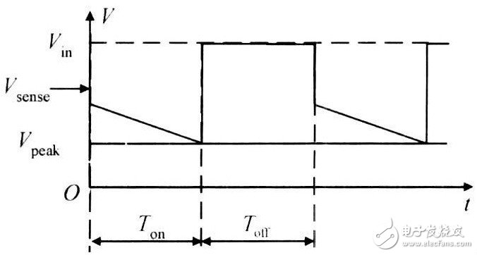
Figure 2 Peak current control process
At the beginning of each cycle, the main RS flip-flop is asserted by the rising edge of the clock, the power switch is turned on, the converter enters the charging phase, the inductor current rises, Isense rises and V sense drops. When the inductor current reaches a peak value, that is, V sense reaches V peak , the output of the current comparator ( Icomp ) resets the RS flip-flop to control the power switch to turn off. This is the working process of the current loop. The peak value of the inductor current is mainly controlled by the voltage loop. Specifically, when the feedback voltage drops below the reference, the error amplifier (EA) output rises, and the V peak voltage that limits the peak of the current rise decreases, so that the duty cycle of the power switch increases, and the output voltage rises, and vice versa. Of course. The feedback voltage is obtained by dividing the output voltage through a resistor.
In the time interval when the power switch is turned off, the conventional step-down Buck converter uses a Schottky diode as a freewheeling diode. Therefore, when the Schottky diode is turned on, the power loss caused by its turn-on voltage drop (typically 013V) will be unavoidable. In order to reduce the conduction loss, a synchronous rectification technique is introduced. Synchronous rectification uses a synchronous power switch instead of a rectifier diode. When the synchronous rectification switch is turned on, the on-resistance is generally below 100mΩ, taking the 1A load as an example. The conduction loss at this time is approximately 011W. For Schottky diodes with a conduction voltage of 013V, the loss is approximately 013W. It can be seen that in the application of small and medium power, synchronous rectification can effectively improve the efficiency of the switching power converter.
Due to the difference in operation between the synchronous rectification switch and the Schottky diode, some control circuits and protection circuits must be introduced at the same time.
First, at the moment when the power switch and the synchronous rectifier switch are switched, a dead time (anTI2shoot2thru) must be set to prevent the two switches from being turned on at the same time, causing the input power to be short-circuited. During the dead time, both the power switch and the synchronous rectification switch are turned off. At this time, the current is freewheeled by the parasitic diode on the synchronous rectification switch. Therefore, the shorter the dead time in a reasonable range, the more power consumption can be reduced. Generally, the design is About 10ns (at 1MHz operating frequency).
Secondly, the synchronous rectification switch is not unidirectionally conductive like the Schottky diode. When the converter operates in the discontinuous current mode, the current on the synchronous rectification switch has dropped to zero and reversed before the start of the next cycle. At this point, the inductor current reversal is equivalent to drawing current from the load, resulting in wasted energy and reduced converter efficiency. Therefore, a detection circuit (rever se) that prevents the reverse current of the synchronous rectification switch must be designed to detect the current direction. This design utilizes the voltage at the SW point. When the voltage changes from negative to positive, the reverse current comparator controls the synchronous rectification switch to turn off.
Sheet Metal Cover,Sheet Metal Frame,Sheet Metal Fabrication Frame,Free Sample Sheet Metal Frame
Dongguan Formal Precision Metal Parts Co,. Ltd , https://www.formalmetal.com