For MAX7456 on-screen display SPI
Abstract: The MAX7456 On-Screen Display (OSD) generator has an SPI â„¢ compatible interface. This application note describes the working principle of the SPI interface. The article also contains the Controller C program that emulates the SPI interface bit by bit in the microcontroller.
The MAX7456 single-channel monochrome on-screen display (OSD) generator is pre-installed with 256 characters and graphics, and can be programmed online via the SPI interface. The working mode, display memory and character memory can be set through the SPI compatible serial interface. The status (STAT) register, display memory data output (DMDO) register, and character memory data output (CMDO) register are all readable and can be written and read. For detailed information about the MAX7456 register and memory structure, refer to the data sheet and application note 4117, "Using the MAX7456 Memory and Evaluation Board Files to Generate Custom Characters and Graphics."
The MAX7456 supports up to 10MHz interface clock (SCLK). Figure 1 shows the timing of writing data, and Figure 2 shows the timing of reading data from the device.
When writing registers, pull / CS low to enable the serial interface. Read data from SDIN on the rising edge of SCLK. When / CS goes high, the data is latched into the input register. If / CS goes high during transmission, the program terminates (ie, data is not written to the register). After / CS goes low, the device waits to read the first byte from SDIN to determine the type of data transfer being performed.
When reading the register, pull / CS low as described above. The address is locked into SDIN on the rising edge of SCLK. Data is then output from SDOUT on the falling edge of SCLK.
The SPI command length is 16 bits: the highest 8 bits (MSB) represent the register address, and the lowest 8 bits (LSB) represent the data (Figures 1 and 2). There are two exceptions to this format:
When performing a read operation, only an 8-bit address is required, as shown in Figure 2. 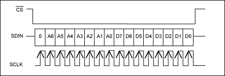
Figure 1. Write operation 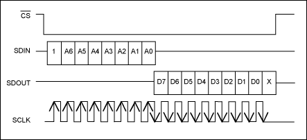
Figure 2. Read operation 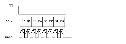
Figure 3. Auto-increment write operation
The C program given below has been compiled for the MAXQ2000 microcontroller for the MAX7456 evaluation (EV) board. This article gives the complete program routine. The program is a readme document with few additional instructions. The C program can be obtained from the following files: spi.c and MAX7456.h.
The following procedure uses the standard definition of the SPI protocol. The MAXQ2000 processor is the SPI master and the MAX7456 is the SPI slave device.
CS is the same as the definition in the MAX7456 data sheet.
SDIN corresponds to MOSI (master out slave device in).
SDOUT corresponds to MOSI (master in and slave out).
SCLK corresponds to CK.
The prefix SPI_ is used for all programs.
The data structure shown below can read or write data directly or bit by bit and is used to access the SPI port independently. C ++ and some newer C compilers support bit-field union / structure statements).
/ * Port 5 Output Register * / __no_init volaTIle __io union {unsigned char PO5; struct {unsigned char bit0: 1; unsigned char bit1: 1; unsigned char bit2: 1; unsigned char bit3: 1; unsigned char bit4: 1; unsigned char bit5: 1; unsigned char bit6: 1; unsigned char bit7: 1;} PO5_bit;} The above code assigns a single byte to PO5, which is the address of the microcontroller output port. Then assign another byte to the same memory address that can be accessed bit by bit.
Therefore, you can directly address the port with the following command:
PO5 = 0x10;
Or use the following command to read and write bit by bit:
PO5_bit.bit4 = 1;
If the program is used for other processors, the structure needs to be rewritten.
If you use an old C compiler that does not support the width of a bit field, you can set and clear the bits using bit Boolean operations:
The following is a simple programming technique to make the program easier to port: Use a macro to define the controller pinout, as shown below.
#define SPI_CS PO5_bit.bit4 // PO5_bit.bit4 = acTIve-low CS—chip select #define SPI_MOSI PO5_bit.bit5 // PO5_bit.bit5 = MOSI—master out slave in, // data to MAX7456 #define SPI_MISO PI5_bit.bit7 / / PO5_bit.bit7 = MISO—master in slave out, // data from MAX7456 #define SPI_CK PO5_bit.bit6 // PO5_bit.bit6 = SCK-SPI clock With the above macro and data structure, each IO port can be set and reset individually, the command is as follows:
SPI_CS = 1;
When the macro is changed, the corresponding pin will also change. When the above code is used in other designs, if the SPI port pin arrangement is different, or the pin is rearranged in order to achieve a more ideal PCB layout, the above program is very useful.
The single-byte write operation (Figure 1) program is shown below. If you can ensure that the state of the / CS and CK lines at the program entry is correct, you can remove the first two commands.
The program first sends the address and then sends the data. Perform two cycles. Using a single cycle and 16-bit data storage can simplify the program. In the MAXQ2000 microcontroller, it takes longer to execute a 16-bit "int" than an 8-bit "char", so there are trade-offs to consider.
The read byte operation (Figure 2) procedure is as follows, similar to the above procedure. Send the address first, then send the clock to read back the data from MISO.
/ ************************************************* ************************************* * spiReadReg * * Reads an 8-bit register with the SPI port. * Data is returned. ******************************************* *********************************************** / unsigned char spiReadReg (const unsigned char regAddr) {unsigned char SPICount; // Counter used to clock out the data unsigned char SPIData; SPI_CS = 1; // Make sure we start with active-low CS high SPI_CK = 0; // and CK low SPIData = regAddr; // Preload the data to be sent with Address and Data SPI_CS = 0; // Set active-low CS low to start the SPI cycle for (SPICount = 0; SPICount <8; SPICount ++) // Prepare to clock out the Address and Data {if (SPIData & 0x80) SPI_MOSI = 1; else SPI_MOSI = 0; SPI_CK = 1; SPI_CK = 0; SPIData << = 1;} // and loop back to send the next bit SPI_MOSI = 0; // Reset the MOSI data line SPIData = 0; for (SPICount = 0; SPICount <8; SPICount ++) // Prepare to clock in the data to be read {SPIData << = 1; // Rotate the data SPI_CK = 1; // Raise the clock to clock the data out of the MAX7456 SPIData + = SPI_MISO; // Read the data bit SPI_CK = 0; // Drop the clock ready for the next bit} // and loop back SPI_CS = 1; // Raise CS return ((unsigned char) SPIData); // Finally return the read data} Write byte operation procedure in auto-increment modeThe procedure for writing bytes in auto-increment mode (Figure 3) is shown below, similar to the single-byte writing procedure described above. Send the address first, then send the clock to read back the data from MISO.
/ ************************************************* ************************************* * spiWriteRegAutoIncr * * Writes to an 8-bit register with the SPI port using the MAX7456's autoincrement mode ******************************************* ******************************************* / void spiWriteRegAutoIncr (const unsigned char regData) {unsigned char SPICount; // Counter used to clock out the data unsigned char SPIData; // Define a data structure for the SPI data. SPI_CS = 1; // Make sure we start with active-low CS high SPI_CK = 0 ; // and CK low SPIData = regData; // Preload the data to be sent with Address and Data SPI_CS = 0; // Set active-low CS low to start the SPI cycle for (SPICount = 0; SPICount <8; SPICount ++ ) // Prepare to clock out the Address and Data {if (SPIData & 0x80) SPI_MOSI = 1; else SPI_MOSI = 0; SPI_CK = 1; SPI_CK = 0; SPIData << = 1;} // and loop back to send the next bit SPI_MOSI = 0; // Reset the MOSI data line} Write the display memory in auto-increment mode SequenceThe program for writing display memory in auto-increment mode is as follows. The program uses a global variable array called "data". The definition is as follows:
extern volatile unsigned char data [DATA_BUF_LENGTH]; DATA_BUF_LENGTH = 968When calling the program, data [] contains the contents of the display memory in the following format:
data [0] = ignored (contains a command byte used by the EV kit GUI software) data [1] = character byte 1 data [2] = attribute byte 1 data [3] = character byte 2 data [4] = attribute byte 2 etc.The auto-increment mode ends by writing 0xFF, so 0xFF cannot be written to the display register in this mode. If you need to write OxFF, you can use a single byte write instruction.
/ ************************************************* ************************************* * spiWriteCM * * Writes to the Display Memory (960 bytes) from "data" extern. * 960 = 16 rows × 30 columns × 2 planes {char vs. attr} screen-position-indexed memory ********************* ************************************************** *************** / void spiWriteCM () // On entry: global data [1..960] // contains char + attr bytes // (optionally terminated by 0xFF data) / / First, write data [1,3,5, ...] Character plane; // MAX7456 WriteReg (0x05,0x41) // "Character Memory Address High"; // 0x02: Attribute bytes; // 0x01: character memory address msb {volatile unsigned int Index = 0x0001; // Index for lookup into // data [1..960] spiWriteReg (DM_ADDRH_WRITE, 0x00); // initialise the Display Memory high-byte spiWriteReg (DM_ADDRL_WRITE, 0x00); // and the low-byte spiWriteReg (DM_MODE_WRITE, 0x41); // MAX7456 WriteReg (0x04,0x41) "Display Memory Mode"; // 0x40: Perform 8-bit operation; 0x01: AutoIncrement Do // Lo op to write the character data {if (data [Index] == 0xFF) {// Check for the break character break;} // and finish if found spiWriteRegAutoIncr (data [Index]); // Write the character Index + = 2; // Increment the index to the next character, // skipping over the attribute} while (Index <0x03C1); // 0x03C1 = 961 // and loop back to send the next character spiWriteRegAutoIncr (0xFF); // Write the "escape character" to end AutoIncrement // mode spiWriteReg (DM_ADDRH_WRITE, 0x02); // Second, write data [2,4,6, ...] // Attribute plane; MAX7456 // WriteReg (0x05,0x41) // "Character Memory Address High"; // 0x02: Attribute bytes; 0x01: character memory address // msb spiWriteReg (DM_ADDRL_WRITE, 0x00); spiWriteReg (DM_MODE_WRITE, 0x41); // MAX7456 WriteReg (0x04,0x41) "Character Memory // Mode "; 0x40: Perform 8-bit operation; 0x01: Auto- // Increment Index = 0x0002; do {if (data [Index] == 0xFF) break; spiWriteRegAutoIncr (data [Index]); Index + = 2;} while (Index <0x03C1); spiWriteRegAutoIncr (0xFF);} write Memory program The procedure for writing a character to the character memory is as follows, each character occupies 18 lines, each line is 12 pixels, a total of 216 pixels. Since each byte defines 4 pixels, 54 bytes are required to define each character. The character data is located in data [] at the entry of the program (similar to the above program for writing display memory).
Some additional instructions are required when writing character memory. The memory is non-volatile, so writing the memory takes about 12ms, which is performed by the MAX7456. Only full 54-byte characters can be written to the character memory.
The device contains a 54-byte mapped memory. First write the character data to be written into the mapping memory, and then the device loads the data into the NVM character memory.
There are several types of registers used to write character memory:
At the program entry, data [1] includes the address of the character to be written, and data [2 ... 54] includes the character data.
When writing characters to the NVM character memory, first write the character address. Then write each byte to the mapped memory. There is no auto-increment mode when writing to the mapped memory, so each write operation must write to the mapped memory address. Writing 0xA0 to the character memory mode register can load the contents of the mapped memory into the NVM character memory. The device then sets bit 5 of the status register high, indicating that it cannot write to character memory. Upon completion, the device resets this bit to low. When the data is moved from the map memory to the character memory, the map memory cannot be written.
To avoid flickering of the display, the program disabled the OSD before writing the character memory.
The header file of the MAX7456 is listed below. The following code determines the register map of the device.
/ ************************************************* ************************************* * spiWriteRegAutoIncr * * Writes to an 8-bit register with the SPI port by using the MAX7456's autoincrement mode ****************************************** ************************************************ // // MAX7456 VIDEO_MODE_0 register #define VIDEO_MODE_0_WRITE 0x00 #define VIDEO_MODE_0_READ 0x80 #define VIDEO_MODE_0_40_PAL 0x40 #define VIDEO_MODE_0_20_NoAutoSync 0x20 #define VIDEO_MODE_0_10_SyncInt 0x10 #define VIDEO_MODE_0_08_EnOSD 0x08 #define VIDEO_MODE_0_04_UpdateVsync 0x04 #define VIDEO_MODE_0_02_Reset 0x02 #define VIDEO_MODE_0_01_EnVideo 0x01 // VIDEO MODE 0 bitmap #define NTSC 0x00 #define PAL 0x40 #define AUTO_SYNC 0x00 #define EXT_SYNC 0x20 #define INT_SYNC 0x30 #define OSD_EN 0x08 #define VERT_SYNC_IMM 0x00 #define VERT_SYNC_VSYNC 0x04 #define SW_RESET 0x02 #define BUF_EN 0x00 #define BUF_DI_DE_DE_1_MODE_VIDEO_MAX_1 81 // MAX7456 DM_MODE register #define DM_MODE_WRITE 0x04 #define DM_MODE_READ 0x84 // MAX7456 DM_ADDRH register #define DM_ADDRH_WRITE 0x05 #define DM_ADDRH_READ 0x85 // MAX7456 DM_ADDRL register #define DM_ADDRL_WRITE 0x06 # def_def_dm # define DM_CODE_IN_READ 0x87 // MAX7456 DM_CODE_OUT register #define DM_CODE_OUT_READ 0xB0 // MAX7456 FM_MODE register #define FM_MODE_WRITE 0x08 #define FM_MODE_READ 0x88 // MAX7456 FM_ADDRH register #define FM_ADDRH_WRITE 0x09 #define #define_define 0x8A // MAX7456 FM_DATA_IN register #define FM_DATA_IN_WRITE 0x0B #define FM_DATA_IN_READ 0x8B // MAX7456 FM_DATA_OUT register #define FM_DATA_OUT_READ 0xC0 // MAX7456 STATUS register #define STATUS_READ 0xA0 #define STATUS_40_RESET_BUSY 0x40 #define STATUS_20_NVRAM_BUSY 0x20 #define STATUS_04_LOSS_OF_SYNC 0x04 #define STATUS_02_PAL_DETECTED 0x02 #de fine STATUS_01_NTSC_DETECTED 0x01 // MAX7456 requires clearing OSD Black Level // register bit 0x10 after reset #define OSDBL_WR 0x6C #define OSDBL_RD 0xEC #define OSDBL_10_DisableAutoBlackLevel 0x10 Conclusion and performanceThe MAX7456 evaluation board uses a MAXQ2000 microcontroller operating at a 20MHz clock, which includes an internal hardware SPI controller. Therefore, the MAX7456's SPI port can work at full speed. The above software SPI program works slower than the hardware controller. However, the program has been optimized to the simplest for the working environment where the customer lacks a hardware SPI port.
Long life, large capacity and good shock resistance, Low self-discharge and good discharge performance at low temperature, Strong charging acceptance and quick-charging capability, strong over-discharge resistance and charge retention, Maintenance-free and no acod or water for maintenance in usage, Excellent large current discharge performance, and have obvious advantages in startup and climbing, Environmental friendly, Lighter weight and smaller size.
Abl Battery,Lithium Battery,Rechargeable Lithium Battery,Motor Lithium Battery
Delight Eco Energy Supplies Co., Ltd. , https://www.cndelight.com