Abstract: This article describes the clamping, biasing, and AC coupling of video signals, the corresponding appropriate signals, the advantages and disadvantages of dual power supply and single power supply, and why some circuits are more suitable for specific applications.
Why do you need to AC couple the video signal? If you haven't asked this question yet, then you should ask. If the reason is a government order, user designation, or industrial agreement, then your choice is probably correct! In many cases, it is because the system uses a single power supply, making you feel that you must use AC coupling. Perhaps you can also choose dual power supply, because using a single power supply means that the video signal must be AC ​​coupled, which will reduce the video quality.
Therefore, before making further decisions, let's look at some actual situations. The single power supply circuit is powered by a single power supply, such as a digital-to-analog converter (DAC). The output of the DAC can be level-converted (a DC operating mode) to ensure that the output is in a dynamic range above ground level. In a specific implementation, a common misconception is that the op amp can detect signals below ground level, so the signal can be reproduced in the output. This view is incorrect. The integrated single power solution is the real solution, but the industry will have to accept the DC offset level of the video output, which is similar to SCART in Europe (SCART is an industry standard for audiovisual equipment interconnection developed by French company Peritel).
Of course, the AC coupling of the video signal poses a problem. The DC level of the signal must be reconstructed after setting the image brightness, and ensure that the signal falls within the linear working area of ​​the next stage. This operation is called "offset", and different circuits can be used depending on the video signal waveform and the required accuracy and stability of the offset point. Sine wave signals such as audio signals can use resistance-capacitance (RC) coupling to establish a stable bias voltage.
Unfortunately, in S video only the chrominance signal (C) approximates a sine wave. Brightness (Y), composite signal (Cvbs) and RGB are complex waveforms, which change from a reference level in one direction, and a synchronization waveform can be superimposed below the reference level. This signal requires a bias method specifically for video signals, called clamping, because it "clamps" one extreme value of the signal at the reference voltage, while the other extreme value can still be changed. The classic form is diode clamping, where the diode is activated by the video's synchronization signal. But there are other forms of clamping.
For example, color-difference signals (Pb and Pr) and graphic RGB signals are better processed with "keyed clamping". This circuit replaces the diode with a switch, which can be externally controlled and uses an external (timing) signal to clamp the video. The last offset method, called "DC recovery", adds feedback to the keyed clamp to improve the offset point accuracy before the analog-to-digital converter (ADC).
Video signal AC coupling When the signal is AC coupled, the coupling capacitor stores the sum of the (signal) average value and the DC potential difference between the signal source and the load. Figure 1 is used to illustrate the effect of AC coupling on the stability of different signal bias points. Figure 1 shows the difference when the sine wave and pulse are AC coupled to a grounded resistance load.
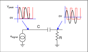
Figure 1. Simple RC coupling for sine waves and pulses to obtain different offset points
At the beginning, both signals change around the same voltage. But after passing the capacitor, different results were obtained. The sine wave changes around the half-amplitude point, while the pulse changes around the voltage as a function of duty cycle. This means that if AC coupling is used, pulses with varying duty cycles will require a wider dynamic range than sine waves of the same amplitude frequency. Therefore, all amplifiers used for pulse signals are best DC coupled to maintain dynamic range. Video signals are similar to pulse waveforms and are also suitable for DC coupling.
Figure 2 shows common video signals and the standard amplitude at the video interface (see EIA 770-1, 2 and 3). The chrominance in S video and Pb and Pr in component video are similar to the sine wave changing around the reference point, as described above. The brightness (Y), composite signal and RGB only change positively from 0V (called "black" or "blanking" level) to + 700mV. Here, the industry's tacit agreement is used instead of any standard. Please note that these signals are complex waveforms with synchronization intervals, although the synchronization interval may not be defined or used. For example, Figure 2 shows RGB with a sync head used in NTSC and PAL. In PC (graphics) applications, synchronization is a separate signal, not superimposed with RGB. In single-supply applications, such as DAC output, the static level may be different during the synchronization interval. This will affect the selection of the bias method. For example, in a dual-supply application, the static level of chroma in the sync interval is not 0V, then the chroma signal will be closer to a pulse than a sine wave.
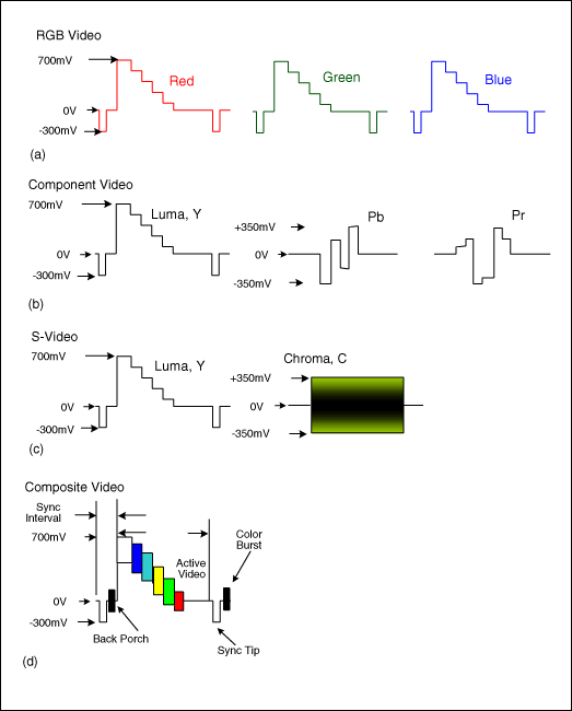
Figure 2. RGB (a), component (b), S-video (c), and composite (d) video signals used to illustrate sync interval, effective video, sync header, and trailing edge.
Despite the above complex factors, the video signal still needs to be AC-coupled to the position where the voltage changes. There is a great danger in the circuit connecting two different power sources through DC coupling, which is strictly prohibited in the safety rules. The manufacturer has a tacit rule that the video signal input is AC-coupled, and the video output is DC-coupled to the next stage to re-establish the DC component, please refer to EN 50049-1 (PAL / DVB [SCART]) and SMPTE 253M Chapter 9.5 (NTSC), allows to provide DC output level. If such a protocol cannot be established, it will lead to "double coupling", that is, two coupling capacitors appear in series, or cause a short circuit, that is, there is no capacitor. The only exception to this rule is battery-powered devices, such as camcorders and cameras, which use AC-coupled outputs to reduce battery consumption.
The next question is how large should this coupling capacitor be? In Figure 1, the assumption that the capacitor stores the "average voltage" of the signal is based on the RC product being greater than the minimum period of the signal. To ensure accurate averaging, the low -3dB point of the RC network must be 6 to 10 times lower than the lowest frequency of the signal. However, this will result in a wide range of capacitance values.
For example, the chroma in S-video is a phase-modulated sine wave with a minimum frequency of about 2MHz. Even with a 75Ω load, only 0.1µF is required unless the horizontal sync interval needs to be passed. In contrast, the frequency response of Y (brightness), Cvbs (composite signal) and RGB extends down to the video frame rate (25Hz to 30Hz). Assuming a 75Ω load and a -3dB point from 3Hz to 5Hz, this requires a capacitance greater than 1000µF. Using too small a capacitor will cause the display image to become darker from left to right and from top to bottom, and may cause spatial distortion of the image (depending on the capacitance). In the video, this is called line bending and field tilt. In order to avoid visible artifacts, its level must be less than 1% to 2%.
The single-supply bias circuit for video is shown in Figure 3a. As long as the RC product is large enough, RC coupling is effective for any video signal. In addition, the corresponding power supply range of the op amp must be sufficient to handle the negative and positive offsets around the average value of the signal. In the past, this was achieved by using dual power supplies for the op amp. Assuming that RS and Ri are referenced to the same ground and are equal to the parallel value of Ri and Rf, the op amp can suppress common mode noise (ie, have a higher common mode rejection ratio [CMRR]) and have the smallest offset voltage. The low -3dB point is 1 / (2¹RSC), and regardless of the size of the coupling capacitor, the circuit can maintain its power supply rejection ratio (PSRR), CMRR, and dynamic range. The vast majority of video circuits are constructed using this method, and the vast majority of AC-coupled video applications still use this method.
With the advent of digital video and battery-powered devices, negative power supplies have become a burden to reduce costs and power consumption. Early attempts at RC biasing were similar to Figure 3b, where a voltage divider was used. Assuming R1 = R2 in Figure 3a, and VCC is equal to the sum of VCC and VEE, these two circuits are similar. But the communication performance of the two is different. For example, any change in VCC in Figure 3b will directly cause the input voltage of the op amp to change according to a certain voltage divider ratio, while in Figure 3a, this change is absorbed by the power supply margin of the op amp. When R1 = R2, the PSRR of Figure 3b is only -6dB. Therefore, the power supply must be filtered and well regulated.
To improve AC PSRR (Figure 3c), inserting an isolation resistor (RX) is a low-cost alternative. However, unless it matches the parallel value of Rf and Ri, this method will bring additional DC offset. Even more troublesome, it also requires that the product of RxC1 and C2Ri must be less than 3 Hz to 5 Hz, as described above. Although the larger bypass capacitor (C3) in this circuit requires a smaller RX and reduces the offset voltage, it also increases C1. This method can be used in low-cost designs that use electrolytic capacitors.
Another option is Figure 3d, which replaces the voltage divider with a 3-terminal regulator and extends PSRR down to DC. The low output impedance of the regulator reduces the offset voltage of the circuit while bringing RX closer to the parallel value of Rf and Ri. Because the sole purpose of C3 is to reduce the regulator noise and compensate the regulator's output impedance (Zout) as a function of frequency, its value is less than the value in Figure 3c. However, C1 and C2 are still very large, and for frequencies lower than the product of RiC1, CMRR has a big problem, and there are also stability problems.
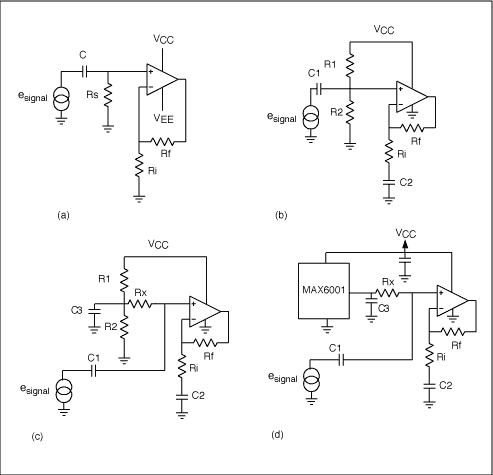
Figure 3. RC bias technology, including dual power supplies (a), a single power supply using a voltage divider (b), a low offset voltage divider (c), and a PSRR-improved voltage regulator source (d).
According to the above, dual-supply AC coupling is better than the single-supply method (considering common-mode rejection and power supply rejection) —regardless of the specific application.
The video clamped brightness, composite signal and RGB signal vary between the black (0V) reference level and the maximum value (+ 700mV) with sync head (-300mV). However, similar to the pulses with varying duty cycles in Figure 1, if these signals are AC-coupled, the bias voltage will vary with the video content (called the average picture level or APL), and brightness information will be lost. A circuit is required to keep the black level constant and not change with the change of the video signal or the amplitude of the sync head.
The circuit shown in Figure 4a is called diode clamping and attempts to be implemented by replacing the resistor with a diode (CR). This diode is equivalent to a unidirectional switch. In this way, most of the negative voltage and horizontal sync of the video signal are forced to ground. Therefore, this circuit is also called sync head clamp. Assuming that the synchronization voltage (-300mV) does not change, and the diode's turn-on voltage is zero, this will keep the reference level (0V) constant. Although the synchronization level cannot be controlled, the turn-on voltage can be reduced, that is, "active clamping" is achieved by placing the clamping diode in the feedback loop of the op amp. The main problem with this is that if the matching circuit is incorrect, it may generate self-excitation, and it is rarely used in discrete designs. The integrated solution can be compensated and has higher reliability. (For example, MAX4399 and MAX4090.)
If the synchronization level changes or does not exist, the diode can be replaced with a switch—usually an FET controlled by an external signal is used (Figure 4b). This is the keyed clamp, and the control signal is the keyed signal. The keying signal is consistent with the synchronization pulse, which achieves synchronization clamping. Unlike diode clamping, this method can be enabled at any position of the sync interval, not just at the sync head. If the keying signal appears when the video signal is black level (Figure 4c), then "black level clamping" is obtained. This method is the most versatile and close to the ideal model. The switch does not have the diode turn-on voltage, and it can truly achieve black level clamping.
Add a DC voltage source (Vref) to set the bias for chroma, Pb and Pr, and composite and luminance signals. The disadvantage is that it requires a synchronous isolator to obtain the keying signal, which is not accurate enough in some applications. If you are quantizing a video signal, you want to keep the black level at ± 1 least significant bit (LSB) or within ± 2.75mV. Clamping cannot achieve such accuracy.
Another method used to provide bias to the video signal is called DC recovery, which can achieve a black level accuracy close to ± 1 LSB. The first point to note in Figure 4d is that there is no coupling capacitor in this circuit. Instead, U2 is used to compare the DC output of the first stage (U1) with a certain voltage (Vref) and apply negative feedback to U1 to force the output to track that voltage regardless of the input voltage. Obviously, if the loop runs continuously, you will get a DC level. A switch can be inserted in the feedback loop. The switch is only momentarily closed at the point where each line needs to be set to Vref (sync head or black level). This voltage is stored by the capacitor (C), but the capacitor is not connected in series with the input, but appears in the form of sample-and-hold (S / H) by switching the feedback loop.
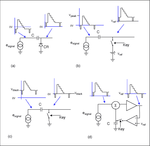
Figure 4. Different forms of video clamping: a) diode or sync head clamp; b) keyed clamp with reference voltage used as sync head clamp; c) keyed clamp used as black level clamp Bit; d) DC recovery
The implementation circuit of Figure 5 is actually composed of two capacitors (Chold and Cx), two op amps (U1 and U2), and an S / H. The real comparison and signal averaging are done by Rx, Cx and U2. The RC product is selected according to the noise average. For a 16ms field signal (NTSC / PAL), the RC product should be greater than 200ns. Therefore, U2 is a low-frequency device selected based on low offset voltage / current and stability, rather than its frequency response characteristics. (MAX4124 / 25 is a good choice for this application.) On the other hand, U1 chooses based on its frequency response, not offset. The selection of S / H and Chold itself depends on its leakage characteristics, that is, the voltage change (drop) caused in each row. The circuit in the figure uses dual power supply, the circuit can also use precise level conversion, and use a single power supply.
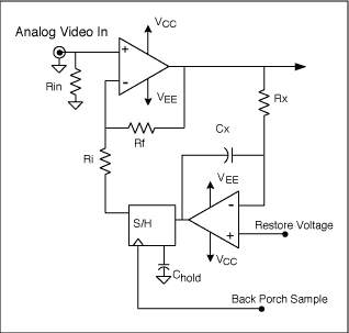
Figure 5. Implementation of a DC recovery circuit using two capacitors, two op amps, and one S / H
The biggest problem with DC restoration is that the restored level—the Vref black video level—is an analog quantity, independent of its value in the digital domain. In order to make corrections, it is usually the same as keyed clamping, which uses DAC to generate Vref. DC recovery can be used for any video signal (with or without synchronization) and can be enabled at any position of the waveform—sufficient for amplifiers and S / H Quick response.
Why do you need to AC couple the video signal? If you haven't asked this question yet, then you should ask. If the reason is a government order, user designation, or industrial agreement, then your choice is probably correct! In many cases, it is because the system uses a single power supply, making you feel that you must use AC coupling. Perhaps you can also choose dual power supply, because using a single power supply means that the video signal must be AC ​​coupled, which will reduce the video quality.
Therefore, before making further decisions, let's look at some actual situations. The single power supply circuit is powered by a single power supply, such as a digital-to-analog converter (DAC). The output of the DAC can be level-converted (a DC operating mode) to ensure that the output is in a dynamic range above ground level. In a specific implementation, a common misconception is that the op amp can detect signals below ground level, so the signal can be reproduced in the output. This view is incorrect. The integrated single power solution is the real solution, but the industry will have to accept the DC offset level of the video output, which is similar to SCART in Europe (SCART is an industry standard for audiovisual equipment interconnection developed by French company Peritel).
Of course, the AC coupling of the video signal poses a problem. The DC level of the signal must be reconstructed after setting the image brightness, and ensure that the signal falls within the linear working area of ​​the next stage. This operation is called "offset", and different circuits can be used depending on the video signal waveform and the required accuracy and stability of the offset point. Sine wave signals such as audio signals can use resistance-capacitance (RC) coupling to establish a stable bias voltage.
Unfortunately, in S video only the chrominance signal (C) approximates a sine wave. Brightness (Y), composite signal (Cvbs) and RGB are complex waveforms, which change from a reference level in one direction, and a synchronization waveform can be superimposed below the reference level. This signal requires a bias method specifically for video signals, called clamping, because it "clamps" one extreme value of the signal at the reference voltage, while the other extreme value can still be changed. The classic form is diode clamping, where the diode is activated by the video's synchronization signal. But there are other forms of clamping.
For example, color-difference signals (Pb and Pr) and graphic RGB signals are better processed with "keyed clamping". This circuit replaces the diode with a switch, which can be externally controlled and uses an external (timing) signal to clamp the video. The last offset method, called "DC recovery", adds feedback to the keyed clamp to improve the offset point accuracy before the analog-to-digital converter (ADC).
Video signal AC coupling When the signal is AC coupled, the coupling capacitor stores the sum of the (signal) average value and the DC potential difference between the signal source and the load. Figure 1 is used to illustrate the effect of AC coupling on the stability of different signal bias points. Figure 1 shows the difference when the sine wave and pulse are AC coupled to a grounded resistance load.
Figure 1. Simple RC coupling for sine waves and pulses to obtain different offset points
At the beginning, both signals change around the same voltage. But after passing the capacitor, different results were obtained. The sine wave changes around the half-amplitude point, while the pulse changes around the voltage as a function of duty cycle. This means that if AC coupling is used, pulses with varying duty cycles will require a wider dynamic range than sine waves of the same amplitude frequency. Therefore, all amplifiers used for pulse signals are best DC coupled to maintain dynamic range. Video signals are similar to pulse waveforms and are also suitable for DC coupling.
Figure 2 shows common video signals and the standard amplitude at the video interface (see EIA 770-1, 2 and 3). The chrominance in S video and Pb and Pr in component video are similar to the sine wave changing around the reference point, as described above. The brightness (Y), composite signal and RGB only change positively from 0V (called "black" or "blanking" level) to + 700mV. Here, the industry's tacit agreement is used instead of any standard. Please note that these signals are complex waveforms with synchronization intervals, although the synchronization interval may not be defined or used. For example, Figure 2 shows RGB with a sync head used in NTSC and PAL. In PC (graphics) applications, synchronization is a separate signal, not superimposed with RGB. In single-supply applications, such as DAC output, the static level may be different during the synchronization interval. This will affect the selection of the bias method. For example, in a dual-supply application, the static level of chroma in the sync interval is not 0V, then the chroma signal will be closer to a pulse than a sine wave.
Figure 2. RGB (a), component (b), S-video (c), and composite (d) video signals used to illustrate sync interval, effective video, sync header, and trailing edge.
Despite the above complex factors, the video signal still needs to be AC-coupled to the position where the voltage changes. There is a great danger in the circuit connecting two different power sources through DC coupling, which is strictly prohibited in the safety rules. The manufacturer has a tacit rule that the video signal input is AC-coupled, and the video output is DC-coupled to the next stage to re-establish the DC component, please refer to EN 50049-1 (PAL / DVB [SCART]) and SMPTE 253M Chapter 9.5 (NTSC), allows to provide DC output level. If such a protocol cannot be established, it will lead to "double coupling", that is, two coupling capacitors appear in series, or cause a short circuit, that is, there is no capacitor. The only exception to this rule is battery-powered devices, such as camcorders and cameras, which use AC-coupled outputs to reduce battery consumption.
The next question is how large should this coupling capacitor be? In Figure 1, the assumption that the capacitor stores the "average voltage" of the signal is based on the RC product being greater than the minimum period of the signal. To ensure accurate averaging, the low -3dB point of the RC network must be 6 to 10 times lower than the lowest frequency of the signal. However, this will result in a wide range of capacitance values.
For example, the chroma in S-video is a phase-modulated sine wave with a minimum frequency of about 2MHz. Even with a 75Ω load, only 0.1µF is required unless the horizontal sync interval needs to be passed. In contrast, the frequency response of Y (brightness), Cvbs (composite signal) and RGB extends down to the video frame rate (25Hz to 30Hz). Assuming a 75Ω load and a -3dB point from 3Hz to 5Hz, this requires a capacitance greater than 1000µF. Using too small a capacitor will cause the display image to become darker from left to right and from top to bottom, and may cause spatial distortion of the image (depending on the capacitance). In the video, this is called line bending and field tilt. In order to avoid visible artifacts, its level must be less than 1% to 2%.
The single-supply bias circuit for video is shown in Figure 3a. As long as the RC product is large enough, RC coupling is effective for any video signal. In addition, the corresponding power supply range of the op amp must be sufficient to handle the negative and positive offsets around the average value of the signal. In the past, this was achieved by using dual power supplies for the op amp. Assuming that RS and Ri are referenced to the same ground and are equal to the parallel value of Ri and Rf, the op amp can suppress common mode noise (ie, have a higher common mode rejection ratio [CMRR]) and have the smallest offset voltage. The low -3dB point is 1 / (2¹RSC), and regardless of the size of the coupling capacitor, the circuit can maintain its power supply rejection ratio (PSRR), CMRR, and dynamic range. The vast majority of video circuits are constructed using this method, and the vast majority of AC-coupled video applications still use this method.
With the advent of digital video and battery-powered devices, negative power supplies have become a burden to reduce costs and power consumption. Early attempts at RC biasing were similar to Figure 3b, where a voltage divider was used. Assuming R1 = R2 in Figure 3a, and VCC is equal to the sum of VCC and VEE, these two circuits are similar. But the communication performance of the two is different. For example, any change in VCC in Figure 3b will directly cause the input voltage of the op amp to change according to a certain voltage divider ratio, while in Figure 3a, this change is absorbed by the power supply margin of the op amp. When R1 = R2, the PSRR of Figure 3b is only -6dB. Therefore, the power supply must be filtered and well regulated.
To improve AC PSRR (Figure 3c), inserting an isolation resistor (RX) is a low-cost alternative. However, unless it matches the parallel value of Rf and Ri, this method will bring additional DC offset. Even more troublesome, it also requires that the product of RxC1 and C2Ri must be less than 3 Hz to 5 Hz, as described above. Although the larger bypass capacitor (C3) in this circuit requires a smaller RX and reduces the offset voltage, it also increases C1. This method can be used in low-cost designs that use electrolytic capacitors.
Another option is Figure 3d, which replaces the voltage divider with a 3-terminal regulator and extends PSRR down to DC. The low output impedance of the regulator reduces the offset voltage of the circuit while bringing RX closer to the parallel value of Rf and Ri. Because the sole purpose of C3 is to reduce the regulator noise and compensate the regulator's output impedance (Zout) as a function of frequency, its value is less than the value in Figure 3c. However, C1 and C2 are still very large, and for frequencies lower than the product of RiC1, CMRR has a big problem, and there are also stability problems.
Figure 3. RC bias technology, including dual power supplies (a), a single power supply using a voltage divider (b), a low offset voltage divider (c), and a PSRR-improved voltage regulator source (d).
According to the above, dual-supply AC coupling is better than the single-supply method (considering common-mode rejection and power supply rejection) —regardless of the specific application.
The video clamped brightness, composite signal and RGB signal vary between the black (0V) reference level and the maximum value (+ 700mV) with sync head (-300mV). However, similar to the pulses with varying duty cycles in Figure 1, if these signals are AC-coupled, the bias voltage will vary with the video content (called the average picture level or APL), and brightness information will be lost. A circuit is required to keep the black level constant and not change with the change of the video signal or the amplitude of the sync head.
The circuit shown in Figure 4a is called diode clamping and attempts to be implemented by replacing the resistor with a diode (CR). This diode is equivalent to a unidirectional switch. In this way, most of the negative voltage and horizontal sync of the video signal are forced to ground. Therefore, this circuit is also called sync head clamp. Assuming that the synchronization voltage (-300mV) does not change, and the diode's turn-on voltage is zero, this will keep the reference level (0V) constant. Although the synchronization level cannot be controlled, the turn-on voltage can be reduced, that is, "active clamping" is achieved by placing the clamping diode in the feedback loop of the op amp. The main problem with this is that if the matching circuit is incorrect, it may generate self-excitation, and it is rarely used in discrete designs. The integrated solution can be compensated and has higher reliability. (For example, MAX4399 and MAX4090.)
If the synchronization level changes or does not exist, the diode can be replaced with a switch—usually an FET controlled by an external signal is used (Figure 4b). This is the keyed clamp, and the control signal is the keyed signal. The keying signal is consistent with the synchronization pulse, which achieves synchronization clamping. Unlike diode clamping, this method can be enabled at any position of the sync interval, not just at the sync head. If the keying signal appears when the video signal is black level (Figure 4c), then "black level clamping" is obtained. This method is the most versatile and close to the ideal model. The switch does not have the diode turn-on voltage, and it can truly achieve black level clamping.
Add a DC voltage source (Vref) to set the bias for chroma, Pb and Pr, and composite and luminance signals. The disadvantage is that it requires a synchronous isolator to obtain the keying signal, which is not accurate enough in some applications. If you are quantizing a video signal, you want to keep the black level at ± 1 least significant bit (LSB) or within ± 2.75mV. Clamping cannot achieve such accuracy.
Another method used to provide bias to the video signal is called DC recovery, which can achieve a black level accuracy close to ± 1 LSB. The first point to note in Figure 4d is that there is no coupling capacitor in this circuit. Instead, U2 is used to compare the DC output of the first stage (U1) with a certain voltage (Vref) and apply negative feedback to U1 to force the output to track that voltage regardless of the input voltage. Obviously, if the loop runs continuously, you will get a DC level. A switch can be inserted in the feedback loop. The switch is only momentarily closed at the point where each line needs to be set to Vref (sync head or black level). This voltage is stored by the capacitor (C), but the capacitor is not connected in series with the input, but appears in the form of sample-and-hold (S / H) by switching the feedback loop.
Figure 4. Different forms of video clamping: a) diode or sync head clamp; b) keyed clamp with reference voltage used as sync head clamp; c) keyed clamp used as black level clamp Bit; d) DC recovery
The implementation circuit of Figure 5 is actually composed of two capacitors (Chold and Cx), two op amps (U1 and U2), and an S / H. The real comparison and signal averaging are done by Rx, Cx and U2. The RC product is selected according to the noise average. For a 16ms field signal (NTSC / PAL), the RC product should be greater than 200ns. Therefore, U2 is a low-frequency device selected based on low offset voltage / current and stability, rather than its frequency response characteristics. (MAX4124 / 25 is a good choice for this application.) On the other hand, U1 chooses based on its frequency response, not offset. The selection of S / H and Chold itself depends on its leakage characteristics, that is, the voltage change (drop) caused in each row. The circuit in the figure uses dual power supply, the circuit can also use precise level conversion, and use a single power supply.
Figure 5. Implementation of a DC recovery circuit using two capacitors, two op amps, and one S / H
The biggest problem with DC restoration is that the restored level—the Vref black video level—is an analog quantity, independent of its value in the digital domain. In order to make corrections, it is usually the same as keyed clamping, which uses DAC to generate Vref. DC recovery can be used for any video signal (with or without synchronization) and can be enabled at any position of the waveform—sufficient for amplifiers and S / H Quick response.
Polyester Tipped Swabs,Cleanroom Polyester Swab,Sterile Polyester Tipped Applicators,Flat Rectangular Head Swab
Miraclean Technology Co., Ltd. , https://www.mrccleanroom.com