Summary:
UV LED light source has the advantages of environmental protection, low power consumption and band selection compared to traditional UV light sources. The application of UV LEDs in the printing industry often faces multiple challenges, with reliability issues being particularly acute. Organic materials have the characteristics of poor UV resistance and high moisture permeability and oxygen permeability, and the deterioration of their performance can greatly reduce the reliability of UV LEDs. 100% of all inorganic UV LEDs based on CMH packaging technology are encapsulated in inorganic materials, which have the advantages of good air tightness, high reliability, long life and low thermal resistance. Due to the difference in COB and DOB modules in packaging materials and production processes, the performance and reliability of the two are quite different. The thermal resistance of the substrate insulation layer accounts for a large proportion of the total thermal resistance of the COB, and the solder interconnection layer has a large influence on the thermal resistance of the DOB. For the problem of excessive voiding of the solder layer between the UV LED device and the substrate during mounting (generally over 20%), the optimal process parameters are obtained through a large number of experiments, and the void ratio of the solder layer can be controlled to 100% or less, and The proportion of voids around 5% is more than 80%, which greatly reduces the influence of the void ratio of the solder layer on the photothermal performance and reliability of the device.
Keywords: UV LED, printing industry, reliability, void rate
I. Introduction
In the 1860s, the first UV-curable ink was introduced. With the rapid development of UV curing technology, UV printing inks have been widely used in the printing industry, such as digital printing, stencil printing, lithography, flexographic printing and gravure printing. The UV curing light source is matched with UV mercury. Traditional light sources such as lights. However, the traditional ultraviolet light source has been restricted by more and more countries for environmental reasons, which makes the market size of Ultra-Violet Light Emitting Diode (UV LED) grow rapidly.
Compared with traditional UV light sources, UV LEDs have many advantages such as energy saving, long life, low power consumption and wavelength selection. According to the wavelength of the light, the UV LED can be divided into long-wave ultraviolet UVA (315~400 nm), medium-wave ultraviolet UVB (280~315 nm) and short-wave ultraviolet UVC (200~280 nm). In general, light-emitting wavelengths greater than 300 nm are shallow ultraviolet, and less than 300 nm are deep ultraviolet. Depending on the package and integration, UV LEDs can be divided into discrete devices and integrated modules, as shown in Table 1. Among them, the integrated module can be divided into COB (Chip On Board) and DOB (Device On Board). The COB is to solder a plurality of LED chips directly on a substrate, and the DOB first encapsulates the LED chips in the device and then solders the plurality of devices on one substrate.
As an emerging light source, UV LEDs also face various challenges when applied to the printing industry. For example, organic materials are exposed to UV energy to produce photodegradation [1]. Overexposure of UV curable inks leads to excessive ink surface or insufficient exposure. Insufficient force [1], harmful substances invade the interior of the UV curing light source, causing the light source to fail, the band matching of the UV curing light source and the UV curing ink, the light uniformity and light extraction efficiency of the UV curing light source, and the life, stability and reliability of the UV curing light source. Wait. At present, the packaging technology level of each LED packaging company is different. There are many types of UV LED light sources on the market and the quality is uneven. This makes the application end often suffer losses due to various reliability problems of the light source. Therefore, this paper studies and discusses the reliability of UV LED in the printing industry from two aspects: UV LED discrete device and UV LED integrated module.

Table 1 Several typical package products of UV LED
Second, UVLED discrete devices
As shown in Table 1, UV LED discrete devices can be classified into organic material package UV LEDs and inorganic material package UV LEDs according to packaging materials. The organic material package UV LED is still packaged by visible light LED devices, that is, a layer of organic packaging materials such as epoxy resin, organic silica gel, etc. is coated on the UV LED chip, or an organic material is used as a bowl for the UV LED device. Cups, such as the EMC series commonly found on the market. Inorganic material package UV LEDs have been improved in packaging methods, generally using ceramics as cups, glass or metallic glass as cover plates. In terms of material properties, organic materials have large differences from inorganic materials. When applied to UV LED packages, the effects of the two materials on the performance, life and reliability of the entire device are also quite different. For the sake of discussion, organic materials are represented by organic silica gel, and inorganic materials are represented by glass. The two are compared in the following aspects.
(1) Transmission rate
The transmittance of the encapsulating material on the chip exit path in the UV band directly affects the light output of the UV LED. The higher the transmittance of the material in the UV band, the higher the light output of the UV LED. Due to the different material properties, the transmittance of different materials in the same UV band will vary greatly. As shown in Figure 1, the initial transmittance of organosilica (methyl silica gel and phenyl silica gel) has no advantage over glass at all wavelengths throughout the UV range. Moreover, as the wavelength decreases, the initial transmittance of the organic silica gel and the glass will decrease to some extent, and the initial transmittance of the organic material decreases more rapidly than the glass. At 300 nm, the initial transmittance of methyl silica gel is already less than 85%, which has a great influence on the light output of the chip, so methyl silica gel is not suitable for the ultraviolet band with a lower band. In addition, after the organic silica gel and the glass were exposed to UV light of 365 nm for 24 hours, the transmittance of the organic silica gel in the UV band was greatly lowered, and the transmittance of the glass was substantially unchanged. It can be seen that in the ultraviolet band, the initial transmittance of the glass and the transmittance after UV aging are superior to those of the organic silica gel.
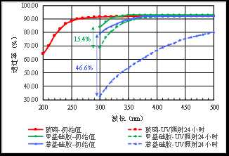
Figure 1. Transmission of typical organic and inorganic materials before and after UV irradiation.
(2) Thermal properties
For UV LEDs encapsulated in organic materials, the organic material is not only exposed to the ultraviolet light emitted by the chip, but also affected by the heat generated by the chip. In particular, the organic material directly coated on the surface of the chip, the high heat of the surface of the chip is directly transferred to the organic material by means of heat conduction, so that the organic material is in a high temperature working state for a long time. The high temperature accelerates the thermal aging of organic materials. If the organic materials used are poor in heat resistance, yellowing is likely to occur, and serious abnormalities such as carbonization (blackening) or cracking may occur. If the device is in a switch or high-temperature cycle for a long period of time, since the chip does not match the coefficient of thermal expansion (CTE) of the organic material, the bond between the chip and the organic material is liable to cause peeling abnormality. Abnormalities such as yellowing and peeling can reduce the light output and reliability of the device.
In order to investigate the heat resistance of organic materials and inorganic materials, methyl silica gel, phenyl silica gel and glass were simultaneously baked in an oven at 260 °C. Appearance inspection found that: phenyl silica gel was found to be obviously yellow on the third day of baking. On the seventh day of baking, methyl silica gel showed crack abnormality despite no obvious yellowing, and the glass did not show any obvious abnormality. The yellowing of phenyl silica gel is because its branched phenyl group is oxidized under high temperature and oxygen environment, and the cracking of methyl silica gel is caused by high temperature to break the bond (chemical bond energy size: Si-O>CH>benzene ring C = C. The larger the chemical bond energy, the harder it is to be destroyed). Since the main component of glass is silica, its chemical stability is excellent. It can be seen that the heat resistance of glass has a great advantage compared to organic silica gel.
(3) Reliability test
It has been found that organic materials undergo photodegradation due to UV irradiation for a long time (photooxidation occurs in an aerobic environment) [1], aging and yellowing occur [3], and severe cracking even occurs [4], making the device light The efficiency and reliability are greatly reduced, eventually leading to failure, which is especially serious in the deep ultraviolet range. To evaluate the reliability level of UV LEDs or the UV resistance of packaging materials, a series of reliability tests are usually performed. Taking the normal temperature aging test as an example, the UV LEDs in the glass package and the methyl silicone package are simultaneously illuminated at a normal ambient temperature (chip wavelength is 395 nm), and radiant flux detection and appearance observation are performed every 48H.
As shown in Figure 2, the radiant flux of the glass-encapsulated UV LED gradually decreases with increasing aging time. The radiant flux at 528H is about 93.1% before aging, and the appearance does not change significantly. The radiant flux of UV-LED encapsulated UV LEDs began to decrease drastically at the beginning of aging, and no obvious abnormalities were observed in the appearance. The main reason was the decrease in transmittance of methyl silica gel and the aging characteristics of the chip (aging). The initial radiant flux value drops faster). As the aging time increases, the rate of decrease of radiant flux begins to decrease. At this time, it is found that cracks have appeared inside the silica gel (mainly distributed near the chip), and the bonding interface between the silica gel and the chip has been peeled off. Figure 3 (left) shows. The appearance of the methyl silica crack indicates that the broken bond has occurred, and the peeling abnormality is due to the mismatch between the thermal expansion coefficient of the silica gel and the chip. Starting at about 336H, the rate of decline of the radiant flux of the UV-gel encapsulated UV LED is significantly increased, and the radiant flux at 528H is about 63.4% before aging. At this time, the appearance inspection found that the silica gel directly above the chip had obvious cracking (as shown in Figure 3 (right)), which is the main reason for the accelerated decline of radiant flux. If the lifetime of the UV LED is defined as the time when the radiant flux is reduced to 70% of the initial value, then the lifetime of the UV-encapsulated UV LED is much shorter than the UV LED of the glass package.
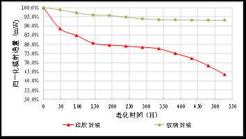
Figure 2 Radiation flux curve of UV LED normal temperature aging for typical organic and inorganic materials
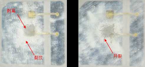
Figure 3. Appearance of a typical organic material package UV LED after normal temperature aging (336H on the left and 528H on the right)
(4) Air tightness
The airtightness of UV LED devices is limited by the moisture permeability and encapsulation level of the packaging materials. The moisture permeability of the encapsulating material is high, and the airtightness of the device is poor. The harmful substances in the external environment easily invade the inside of the device through the encapsulating material and cause device failure. Poor air tightness of the device can cause various reliability problems, such as chip etching and blackening of the silver plating layer.
The oxygen permeability of the organic encapsulating material is higher than that of the glass. For example, the oxygen permeability of methyl silica gel is usually 20,000 to 30,000 cm 3 / (m 2 × 24 H × atm), and the phenyl silica gel is generally 300 to 3000 cm 3 / (m 2 × 24H × atm), generally gas and water can penetrate into the interior of the organic silica gel. Glass is a kind of highly dense inorganic substance, and its intermolecular gap is smaller than water, so generally neither gas nor water can pass through the glass. Therefore, glass is easier to achieve a hermetic package than silicone.
(5) Electrical properties
Organic materials such as organosilica typically contain a certain amount of Na+, K+, and Cl- plasma, and organic materials are more or less free to release small molecules during use. The organic material is coated on the surface of the chip, and the ions inside the organic material or the excessive release of small molecular substances may cause a certain degree of damage to the electrical properties of the chip, such as the generation and increase of reverse leakage current of the chip. This is not the case with glass.
In summary, the properties of inorganic materials are superior to those of organic materials. Organic materials often match near-ultraviolet UV LED chips for applications where performance and reliability are low, and UV LEDs in inorganic materials should be used in harsh environments such as high temperatures and high humidity or other high requirements. All-inorganic UV LED products developed by Guangzhou Hongli Bingyi Optoelectronics Technology Co., Ltd. (structure shown in Figure 4, product performance as shown in Table 2) using CMH full inorganic packaging technology (Ceramic ceramics, Metal metal, Hard glass/quartz Hard glass), that is, ceramic as the substrate, UV LED chip is placed in the cavity of the ceramic substrate, metal and hard glass are used as the cover plate, the cover plate and the substrate are welded, and the cavity is filled with nitrogen gas to form airtightness. The package (the air tightness test passed the US military standard MIL-STD-883). Because it is 100% encapsulated with inorganic materials, the reliability problem caused by the deterioration of organic material performance is completely avoided. Compared with other UV LED devices, all inorganic UV LED devices based on CMH packaging technology have the advantages of low thermal resistance, long life, good air tightness and high reliability, which are suitable for various occasions in the printing industry.
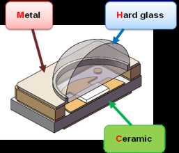
Figure 4 Schematic diagram of the full inorganic UV LED structure based on CMH packaging technology

Table 2 Product Performance Table
Third, UV LED integrated module
As mentioned above, the common UV LED integrated modules currently on the market mainly include COB and DOB. The difference between the two modules is mainly reflected in the following aspects: First, packaging materials; Second, production process; Third, optical performance; Fourth, electrical performance; Fifth, thermal performance.
(1) packaging materials
The main difference between COB and DOB in the choice of package materials is the chip and substrate. At present, COBs using horizontal structure chips and COBs of vertical structure chips are common, and DOB basically uses vertical structure chips. There are two main types of substrates for the UV LED integrated module, namely a copper substrate and an aluminum nitride (AlN) ceramic substrate. The difference between the two substrates is reflected in the following aspects. First, the price. Aluminum nitride ceramic substrates are more expensive than copper substrates. Second, the structure. The structure of the copper substrate is generally a circuit layer (copper layer), an insulating layer (BT resin), and a copper layer from top to bottom, and the aluminum nitride ceramic substrate is generally a circuit layer and a ceramic layer. Third, the mechanical properties. Aluminum nitride ceramics are very brittle and are prone to cracks and even cracks during manufacturing and installation, and copper substrates generally do not exhibit such anomalies. Fourth, thermal performance. Although the thermal conductivity of copper is higher than that of aluminum nitride, the copper substrate contains an insulating layer, which will hinder the heat dissipation of the chip to some extent. Fifth, design diversity. The copper substrate is more susceptible to variations in shape and size than ceramic substrates. The choice of packaging materials will vary, and the performance and reliability of the device will vary.
(2) Production process
Mainly reflected in the following two aspects. 1. COB is generally a customized product, and it is difficult to achieve standardization or large-scale production. DOB is a UV LED device that has been standardized and mass-produced on a substrate. Second, the manufacturing process of COB is more difficult than DOB. Once manufacturing defects occur, such as collapse, the entire COB is scrapped, and DOB only loses a certain device. Moreover, in the event of a light source failure during use, the COB can only replace the entire light source, and the DOB only needs to replace the failed device.
(4) Light performance
Since the lateral structure chip usually uses sapphire as the substrate, its heat dissipation performance is worse than that of the vertical structure chip. Therefore, the vertical structure chip can allow the maximum forward current and optical power density to be larger than that of the lateral structure chip. COBs using laterally structured UV LED chips are often used for low power (below tens of watts) where they are limited by chip characteristics.
(5) Electrical properties
At present, the anti-static protection of UV LEDs is basically realized by the method of Garzina. Therefore, COB cannot achieve anti-static protection for each chip, and DOB can. Therefore, the antistatic performance of COB is much worse than DOB. Moreover, the DOB module can realize the lighting test and leakage current test of a single device through the circuit design of the substrate, which is convenient for failure analysis.
(6) Thermal properties
In general, there are three main heat dissipation paths for UV LED devices: 1 chip - gold wire - circuit layer - bowl cup - environment; 2 chip - outer sealant (gas or air) - lens (cover) - environment; 3 chips - Solid crystal layer - substrate - environment. In contrast, the heat dissipation capabilities of paths 1 and 2 are limited, and path 3 is the primary heat dissipation path. Accordingly, the typical structure and main heat dissipation path of COB and DOB are shown in Figure 5. As mentioned above, the lateral structure chip itself has poor heat dissipation performance. Then, comparing the heat dissipation paths of the COB and DOB using the vertical structure UV LED chip, it can be found that the DOB has two thin gold plating layers and one aluminum nitride ceramic on the device and a layer of solder between the substrate and the device. Layer, but one layer of insulation is missing on the substrate (thermal conductivity is shown in Table 3). The thermal resistance of COB and DOB is calculated without considering the factors such as diffusion thermal resistance. It can be seen from Table 3 that the total thermal resistance of the COB is much larger than that of the DOB because the thermal resistance of the insulating layer in the COB copper substrate is too large. For DOB, the solder interconnect layer (including the solid crystal layer and the solder paste layer) has a large total thermal resistance. If the solder joint quality of the interconnect layer is not good, such as insufficient solder or a large number of voids, the total The effect of thermal resistance will be even greater. Studies have shown that the interconnect quality of the LED interconnect layer has a great impact on the LED light extraction efficiency [5], total thermal resistance [6] and reliability [7]. Among them, for the influence of thermal resistance, Amy S. Fleischer et al. found that the influence of multiple randomly distributed small holes (total percentage V%) on the total thermal resistance (Rjc) of the device is Rjc=0.007V%+1.4987 The influence of multiple relatively large holes on the total thermal resistance of the device is Rjc=1.427e0.015V% [8]. Therefore, the quality of the solder joints of the DOB is critical.

(a) COB using a lateral structure UV LED chip

(b) COB using vertical structure UV LED chips
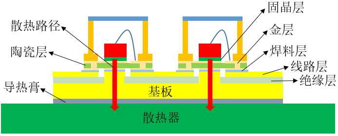
(c) DOB using vertical structure UV LED chips
Figure 5 Typical COB and DOB module structure
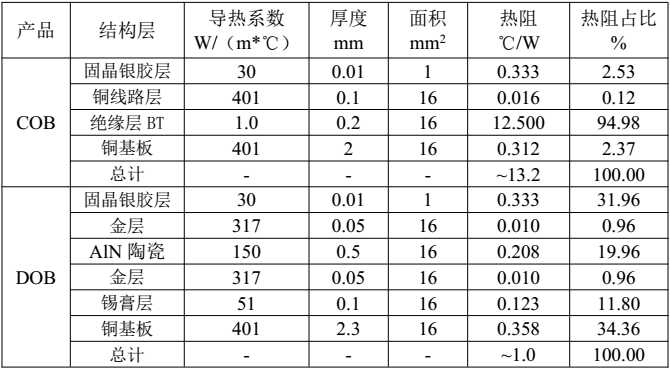
Table 3 Thermal resistance calculation of COB and DOB
Since the die bonding process is mature and the chip area is not large, the soldering quality of the die bond layer is easily controlled. However, for the solder layer between the device and the substrate, due to problems such as large pad area, material properties, and process level, bubbles are inevitably generated to form voids. At present, the void ratio of the solder paste layer of DOB module products in the industry is generally above 20%, as shown in Figure 6.
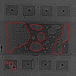
Figure 6 X-RAY scan of a typical DOB module
Guangzhou Hongli Bingyi Optoelectronics Technology Co., Ltd. has done the following research on the control of void rate:
1. Comparison of various solder pastes of different brands;
Second, the stencil design: different thickness, different graphic shapes and different graphic sizes;
Third, the reflow oven process parameters adjustment, including temperature and time.
After a lot of experiments, the optimal process was found. The void rate of the solder paste layer can be controlled within 100% (as shown in Figure 7), and the void ratio of 5% or so is more than 80%. This optimal process is used for device placement of DOB modules, which enables interconnection of low void ratios, thereby greatly reducing the effect of voids on the photothermal characteristics and reliability of UV LED devices.
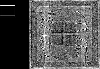
Figure 7 X-RAY scan of a typical DOB module after process optimization
Fourth, summary
By analyzing the two aspects of UV LED discrete devices and integrated modules, inorganic packaging materials are superior to organic packaging materials in terms of transmittance (UV band), air tightness, electrical properties and thermal properties. . Therefore, UV LED devices and modules packaged in organic materials are only suitable for applications where power and lifetime are less demanding, and all inorganic UV LED devices and modules based on CMH packaging technology can be adapted to various occasions in the printing industry. In addition, in view of the large void rate of the DOB module solder paste layer in the industry, the optimal process parameters have been obtained through a large number of experiments. Using this optimal process parameter, the void ratio of the solder paste layer can be controlled to 100% or less, and the void ratio of about 5% is more than 80%, thereby greatly reducing the solder interconnect layer void to the UV LED. The effects of the photothermal characteristics and reliability of the device.

An electrical appliance used to protect electrical equipment from high transient overvoltage hazards and to limit the duration of continuous flow.This term includes any external clearance necessary for the normal functioning of the appliance during operation and installation, whether or not it is a unit as a whole.
Surge protector, also known as lightning arrester, is an electronic device that provides safety protection for all kinds of electronic equipment, instruments and communication lines.When the electric circuit or communication lines or for outside disturbance suddenly produce peak current in voltage, surge protector in a very short time conduction tap, to avoid surge damage to other devices in the circuits.[1]
Surge protector, suitable for ac 50/60 hz, rated voltage 220 v to 380 v power supply system, the indirect lightning and thunder and lightning directly affect transient over voltage surge protection, or other applicable to the family home, the third industry and the surge protection industry requirements.
Surge Protector,Surge Voltage Protector,Eco-Friendly Surge Protector,Lightning Protection Surge Protector
YANGZHOU POSITIONING TECH CO., LTD , https://www.yzpstcc.com