The PIC16F616 is a 14-pin, 8-bit CMOS microcontroller. With a reduced instruction set, there are only 35 instructions. Because of the Harvard bus structure, which uses a separate data bus and instruction bus, most of the instructions are single-cycle instructions except that a small number of instructions are not single-cycle. This is beneficial to improve the operating speed and execution efficiency of the microcontroller.
The PIC16F616 can be powered from 2V to 5.5V. It integrates an RC oscillator with a frequency of 8MHz or 4MHz. It can also be clocked by an external crystal. It integrates hardware modules such as AD conversion and comparator, and also has functions such as power-on reset, undervoltage reset, watchdog, and code protection. Three timers, PWM generators, etc. can be programmed by the user. The following describes the package of the PIC16F616.
The PIC16F616 has a ten-bit, eight-way AD converter. The reference voltage can be considered as the power supply voltage VDD, or it can be an external reference voltage (VREF pin). When the AD conversion is completed, a discontinuity can be generated. This interrupt can wake up the microcontroller from sleep state.
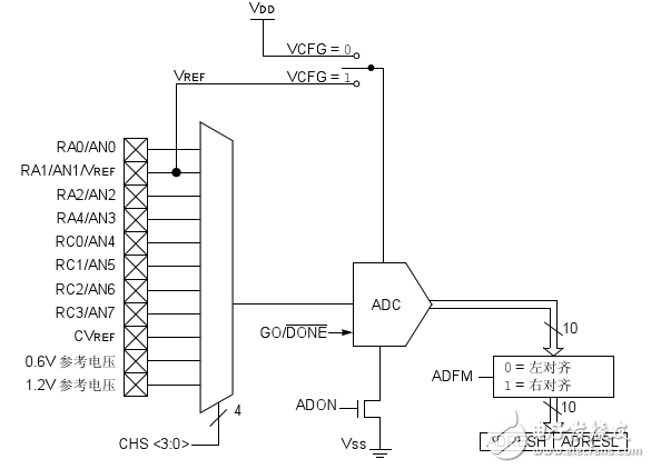
ADC block diagram
ADC configuration1, port configuration
The port that needs to sample the analog signal must be set to the analog input state. If set to a digital port, the conversion result will be inaccurate, and the analog input of the port can be configured by the register ANSEL.
2, channel selection
There are eight external channels and three internal channels. The channel selection can be set by the CHS "3:0" bit in the ADCON0 register.
3, ADC reference voltage
The reference voltage can be either VDD or an external reference voltage, which can be set by the VCFG bit in the ADCON0 register. When VCFG = 0, the reference voltage is VDD. When VCFG = 1, the reference voltage is the external reference voltage (from VREF). foot).
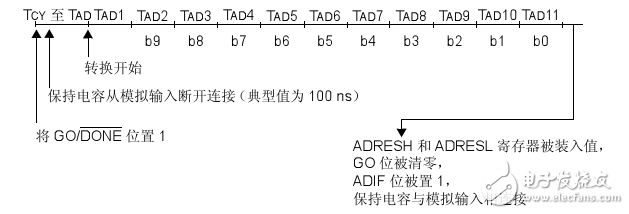
Analog to digital conversion TAD cycle
4, conversion clock
Register ADCON1 is used to set the clock source of AD. ADCS "2:0" can be combined to set the clock source of AD to different frequency. It can be considered as FOSC/2, FOSC/4, FOSC/8, FOSC/16, FOSC. /32, FOSC/64 and FRC (internal RC).
5, interrupt
To use the interrupt function of AD, the AD interrupt enable can be enabled first, the ADIE bit is set to 1 (in register PIE1), the PEIE bit is set (in the INTCON register), and the GIE bit is always set (in the INTCON register).
6, the result format
The result of AD conversion is retained in a register pair: ADRESH and ADRESL, but the AD conversion result is only ten bits. Setting the AD conversion pattern can be selected by setting the ADFM bit of ADCON0. When ADFM=1, the 10-bit AD result is low. Eight bits remain in ADRESL, and the upper two bits remain in ADRESH; when ADFM=0, the upper eight bits of the 10-bit AD result remain in ADRESH, and the lower two bits remain in ADRESL.
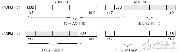
10-bit A/D conversion result format
UV Film,UV Screen Protector,UV Curing Screen Protector
Shenzhen Jianjiantong Technology Co., Ltd. , https://www.jjthydrogelmachine.com